- 您现在的位置:买卖IC网 > PDF目录3709 > MAX13202EALT+T (Maxim Integrated Products)IC ESD PROTECT 2CH 6-UDFN PDF资料下载
参数资料
| 型号: | MAX13202EALT+T |
| 厂商: | Maxim Integrated Products |
| 文件页数: | 5/9页 |
| 文件大小: | 0K |
| 描述: | IC ESD PROTECT 2CH 6-UDFN |
| 产品培训模块: | Lead (SnPb) Finish for COTS Obsolescence Mitigation Program |
| 标准包装: | 1 |
| 电极标记: | 2 通道阵列 - 单向 |
| 安装类型: | 表面贴装 |
| 封装/外壳: | 6-WFDFN |
| 供应商设备封装: | 6-uDFN(1.5x1.0) |
| 包装: | 标准包装 |
| 产品目录页面: | 1424 (CN2011-ZH PDF) |
| 其它名称: | MAX13202EALT+TDKR |
�� �
�
�2-/4-/6-/8-Channel,� ±30kV� ESD� Protectors� in� μDFN�
�During� an� ESD� event,� the� current� pulse� rises� from� zero�
�to� peak� value� in� nanoseconds� (Figure� 3).� For� example,�
�in� a� ±15kV� IEC-61000-4-2� Air-Gap� Discharge� ESD�
�event,� the� pulse� current� rises� to� approximately� 45A� in�
�1ns� (di/dt� =� 45� x� 10� 9� ).� An� inductance� of� only� 10nH� adds�
�an� additional� 450V� to� the� clamp� voltage.� An� inductance�
�of� 10nH� represents� approximately� 0.5in� of� board� trace.�
�Regardless� of� the� device’s� specified� diode� clamp� volt-�
�age,� a� poor� layout� with� parasitic� inductance� significantly�
�increases� the� effective� clamp� voltage� at� the� protected�
�signal� line.�
�A� low-ESR� 0.1μF� capacitor� must� be� used� between� V� CC�
�and� GND.� This� bypass� capacitor� absorbs� the� charge�
�transferred� by� a� +14kV� (MAX13204E/MAX13206E/�
�MAX13208E)� and� ±12kV� (MAX13202E)� IEC61000-4-2�
�Contact� Discharge� ESD� event.�
�Ideally,� the� supply� rail� (V� CC� )� would� absorb� the� charge�
�caused� by� a� positive� ESD� strike� without� changing� its�
�regulated� value.� In� reality,� all� power� supplies� have� an�
�±30kV� ESD� Protection�
�ESD� protection� can� be� tested� in� various� ways.� The�
�MAX13202E/MAX13204E/MAX13206E/MAX13208E� are�
�characterized� for� protection� to� the� following� limits:�
�?� ±15kV� using� the� Human� Body� Model�
�?� ±14kV� (MAX13204E/MAX13206E/MAX13208E)� and�
�±12kV� (MAX13202E)� using� the� Contact� Discharge�
�method� specified� in� IEC� 61000-4-2�
�?� ±30kV� using� the� IEC� 61000-4-2� Air-Gap� Discharge�
�method�
�ESD� Test� Conditions�
�ESD� performance� depends� on� a� number� of� conditions.�
�Contact� Maxim� for� a� reliability� report� that� documents�
�test� setup,� methodology,� and� results.�
�effective� output� impedance� on� their� positive� rails.� If� a�
�power� supply’s� effective� output� impedance� is� 1� ?� ,� then�
�by� using� V� =� I� � R,� the� clamping� voltage� of� V� C� increas-�
�R� C�
�1M� ?�
�R� D�
�1.5k� ?�
�es� by� the� equation� V� C� =� I� ESD� x� R� OUT� .� An� ±8kV�
�IEC� 61000-4-2� ESD� event� generates� a� current� spike� of�
�24A,� so� the� clamping� voltage� increases� by� V� C� =� 24A� �
�1� ?� ,� or� V� C� =� 24V.� Again,� a� poor� layout� without� proper�
�bypassing� increases� the� clamping� voltage.� A� ceramic�
�chip� capacitor� mounted� as� close� to� the� MAX13202E/�
�HIGH-�
�VOLTAGE�
�DC�
�SOURCE�
�CHARGE-CURRENT-�
�LIMIT� RESISTOR�
�Cs�
�100pF�
�DISCHARGE�
�RESISTANCE�
�STORAGE�
�CAPACITOR�
�DEVICE�
�UNDER�
�TEST�
�MAX13204E/MAX13206E/MAX13208E� V� CC� pin� is� the�
�best� choice� for� this� application.� A� bypass� capacitor�
�should� also� be� placed� as� close� to� the� protected� device�
�as� possible.�
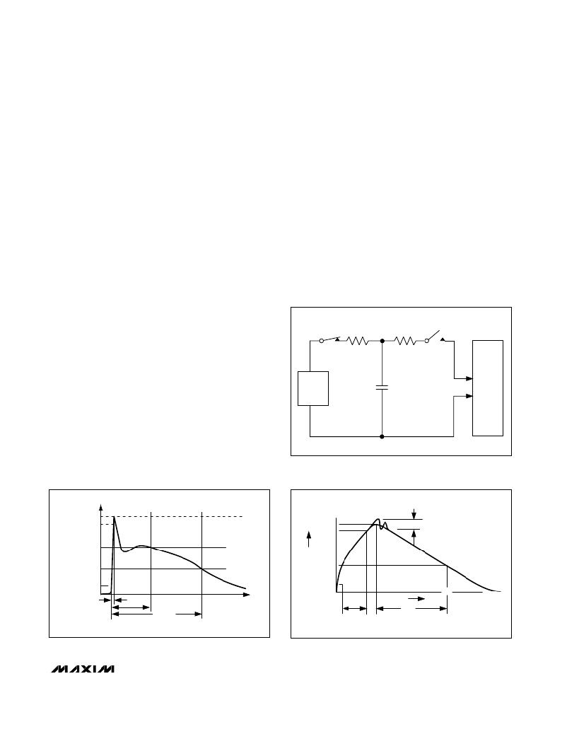
�Figure� 4.� Human� Body� ESD� Test� Model�
�I�
�100%�
�90%�
�I� P� 100%�
�90%�
�Ir�
�PEAK-TO-PEAK� RINGING�
�(NOT� DRAWN� TO� SCALE)�
�AMPERES�
�36.8%�
�10%�
�10%�
�0�
�t� R� =� 0.7ns� to� 1ns�
�30ns�
�60ns�
�t�
�0�
�t� RL�
�TIME�
�t� DL�
�CURRENT� WAVEFORM�
�Figure� 3.� IEC� 61000-4-2� ESD� Generator� Current� Waveform�
�Figure� 5.� Human� Body� Model� Current� Waveform�
�_______________________________________________________________________________________�
�5�
�相关PDF资料 |
PDF描述 |
|---|---|
| 1744037-4 | 04P EC PWR.200 CL HDR ASSY VRT |
| 2029167-4 | CONN PLUG 4POS STR NO DRAIN HOLE |
| MMS-103-01-T-SH | CONN RCPT 2MM 3POS SGL HORZ PCB |
| 929836-01-18-RK | CONN HEADER 36POS DUAL .100 TIN |
| 9-103329-0-23 | CONN HEADR BRKWAY .100 23POS R/A |
相关代理商/技术参数 |
参数描述 |
|---|---|
| MAX13204EALT | 制造商:Maxim Integrated Products 功能描述:LOW-CAPACITANCE 4-/6-/8-CHANNEL + - Rail/Tube |
| MAX13204EALT+ | 制造商:Maxim Integrated Products 功能描述: 制造商:Rochester Electronics LLC 功能描述: |
| MAX13204EALT+T | 功能描述:TVS二极管阵列 4Ch ESD Protection Diode Array RoHS:否 制造商:Littelfuse 极性: 通道:4 Channels 击穿电压: 钳位电压:11.5 V 工作电压:2.5 V 峰值浪涌电流:20 A 安装风格:SMD/SMT 端接类型:SMD/SMT 系列: 最小工作温度:- 40 C 最大工作温度:+ 85 C |
| MAX13204EALT-T | 功能描述:TVS二极管阵列 RoHS:否 制造商:Littelfuse 极性: 通道:4 Channels 击穿电压: 钳位电压:11.5 V 工作电压:2.5 V 峰值浪涌电流:20 A 安装风格:SMD/SMT 端接类型:SMD/SMT 系列: 最小工作温度:- 40 C 最大工作温度:+ 85 C |
| MAX13204EELT+ | 制造商:Rochester Electronics LLC 功能描述: 制造商:Maxim Integrated Products 功能描述: |
发布紧急采购,3分钟左右您将得到回复。