- 您现在的位置:买卖IC网 > PDF目录1835 > MAX13256ATB+T (Maxim Integrated Products)IC TRANSFORMER HBRIDGE 10TDFN PDF资料下载
参数资料
| 型号: | MAX13256ATB+T |
| 厂商: | Maxim Integrated Products |
| 文件页数: | 10/17页 |
| 文件大小: | 0K |
| 描述: | IC TRANSFORMER HBRIDGE 10TDFN |
| 产品培训模块: | Lead (SnPb) Finish for COTS Obsolescence Mitigation Program |
| 标准包装: | 1 |
| 类型: | 半桥 |
| 输入类型: | 非反相 |
| 输出数: | 2 |
| 电流 - 输出 / 通道: | 300mA |
| 电流 - 峰值输出: | 可调式/可编程 |
| 电源电压: | 8 V ~ 36 V |
| 工作温度: | -40°C ~ 125°C |
| 安装类型: | 表面贴装 |
| 封装/外壳: | 10-WFDFN 裸露焊盘 |
| 供应商设备封装: | 10-TDFN-EP(3x3) |
| 包装: | 标准包装 |
| 其它名称: | MAX13256ATB+TDKR |
�� �
�
�MAX13256�
�36V� H-Bridge� Transformer�
�Driver� for� Isolated� Supplies�
�N:1� CT�
�Applications� Information�
�+�
�V� IN�
�-�
�+�
�V� IN�
�-�
�N:1�
�+�
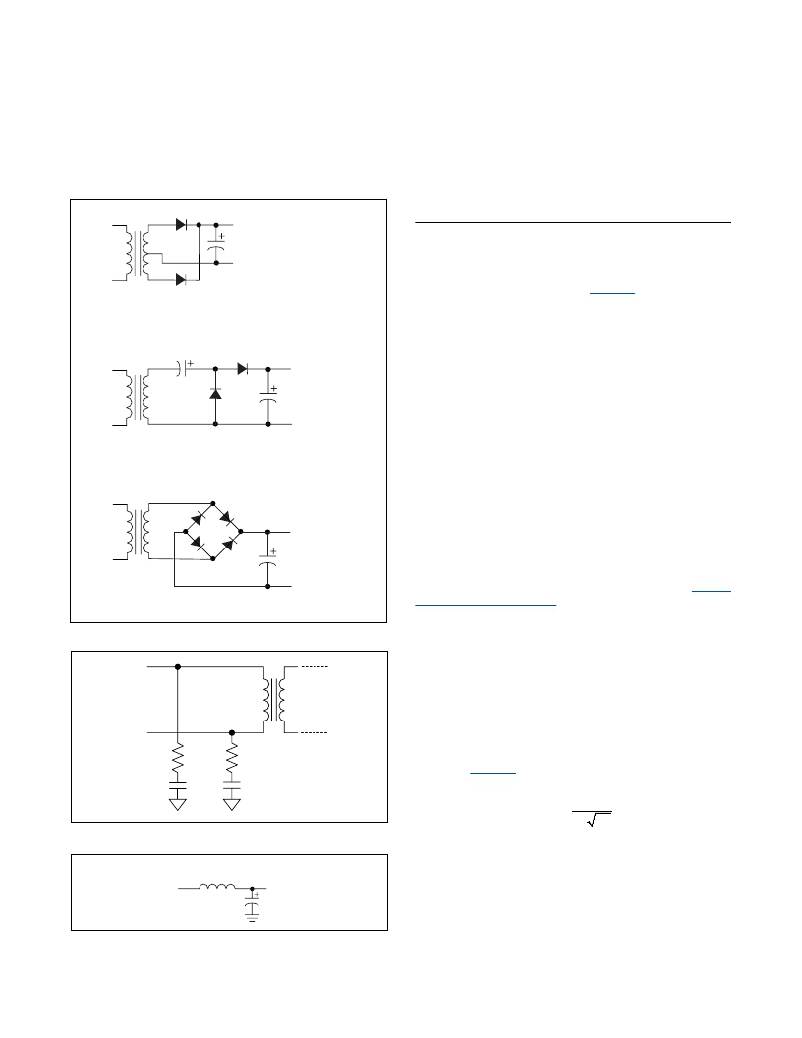
�V� OUT� =� 1/(2� x� N)� x� V� IN� -� V� D�
�-�
�V� D� =� DIODE� FORWARD� VOLTAGE�
�FIGURE� 3A.� PUSH-PULL� RECTIFICATION�
�+�
�V� OUT� =� 2(V� IN� /N� -� V� D� )�
�-�
�FIGURE� 3B.� VOLTAGE� DOUBLER�
�Snubber�
�For� V� DD� greater� than� 27V,� use� a� simple� RC� snubber�
�circuit� on� ST1� and� ST2� to� ensure� that� the� peak� voltage� is�
�less� than� 40V� during� switching� (� Figure� 4� ).� Recommended�
�values� for� the� snubber� are� R� =� 91� I� and� C� =� 330pF.�
�Power� Dissipation�
�The� power� dissipation� of� the� device� is� approximated� by:�
�P� D� =� (R� OHL� x� I� PRI2� )� +� (I� DD� x� V� DD� )�
�where� R� OHL� is� the� combined� high-side� and� low-side� on-�
�resistance� of� the� internal� FET� drivers,� and� IPRI� is� the� load�
�current� flowing� through� ST1� and� ST2.�
�High-Temperature� Operation�
�When� the� MAX13256� is� operated� under� high� ambient�
�temperatures,� the� power� dissipated� in� the� package� can�
�raise� the� junction� temperature� close� to� thermal� shutdown.�
�+�
�V� IN�
�-�
�N:1�
�+�
�V� OUT� =� V� IN� /N� -� 2V� D�
�-�
�Under� such� temperature� conditions,� the� power� dissipa-�
�tion� should� be� held� low� enough� so� that� that� junction� tem-�
�perature� observes� a� factor� of� safety� margin.� The� maximum�
�junction� temperature� should� be� held� below� +140°C.� Use�
�the� package’s� thermal� resistances� to� calculate� the� junc-�
�tion� temperature.� Alternatively� use� the� Maximum� Output�
�Current� vs.� Temperature� curves� shown� in� the� Typical�
�FIGURE� 3C.� FULL-WAVE� RECTIFIER�
�Figure� 3.� Secondary-Side� Rectification� Topologies�
�ST1�
�Operating Characteristics� section� to� determine� the� maxi-�
�mum� ST1/ST2� load� currents.�
�Hot� Insertion�
�If� the� MAX13256� is� inserted� into� a� live� backplane,� it� is�
�possible� to� damage� the� device.� Damage� is� caused� by�
�overshoot� on� V� DD� exceeding� the� absolute� maximum�
�rating.� Limit� the� transient� input� voltage� to� the� MAX13256�
�with� an� external� protection� device.�
�ST2�
�R�
�91� I�
�R�
�91� I�
�Output-Ripple� Filtering�
�Output-voltage� ripple� can� be� reduced� with� a� lowpass� LC�
�filter� (see� Figure� 5� ).� The� component� values� shown� give� a�
�f� 3dB� =�
�C�
�330pF�
�Figure� 4.� Output� Snubber�
�L�
�25μH�
�Figure� 5.� Output� Ripple� Filtering�
�Maxim� Integrated�
�C�
�330pF�
�FILTER�
�OUTPUT�
�C�
�2.2μF�
�cutoff� frequency� of� 21.5kHz� by� the� equation:�
�1�
�2� π� LC�
�Use� an� inductor� with� low� DC� resistance� and� sufficient� sat-�
�uration� current� rating� to� minimize� filter� power� dissipation.�
�Power-Supply� Decoupling�
�Bypass� V� DD� to� ground� with� a� 1� F� F� ceramic� capacitor� as�
�close� as� possible� to� the� device.�
�10�
�相关PDF资料 |
PDF描述 |
|---|---|
| MAX13362ATL/V+T | IC SWITCH 1X2 40TQFN |
| MAX1365ECM+ | IC PANEL METER 4.5 DIG 48LQFP |
| MAX1366ECM+ | IC PANEL METER 4.5 DIG 48LQFP |
| MAX136CPL+ | IC ADC 3 1/2DIG W/LCD DVR 40-DIP |
| MAX14514ETD+T | IC CONV DC-AC EL LAMP 14TDFN |
相关代理商/技术参数 |
参数描述 |
|---|---|
| MAX13256ETB+T | 制造商:Maxim Integrated Products 功能描述: |
| MAX13256EVKIT# | 功能描述:电源管理IC开发工具 36V Transformer Driver RoHS:否 制造商:Maxim Integrated 产品:Evaluation Kits 类型:Battery Management 工具用于评估:MAX17710GB 输入电压: 输出电压:1.8 V |
| MAX1325ECM | 功能描述:模数转换器 - ADC RoHS:否 制造商:Texas Instruments 通道数量:2 结构:Sigma-Delta 转换速率:125 SPs to 8 KSPs 分辨率:24 bit 输入类型:Differential 信噪比:107 dB 接口类型:SPI 工作电源电压:1.7 V to 3.6 V, 2.7 V to 5.25 V 最大工作温度:+ 85 C 安装风格:SMD/SMT 封装 / 箱体:VQFN-32 |
| MAX1325ECM+ | 功能描述:模数转换器 - ADC 14-Bit 4Ch 526ksps 3V Precision ADC RoHS:否 制造商:Texas Instruments 通道数量:2 结构:Sigma-Delta 转换速率:125 SPs to 8 KSPs 分辨率:24 bit 输入类型:Differential 信噪比:107 dB 接口类型:SPI 工作电源电压:1.7 V to 3.6 V, 2.7 V to 5.25 V 最大工作温度:+ 85 C 安装风格:SMD/SMT 封装 / 箱体:VQFN-32 |
| MAX1325ECM+T | 功能描述:模数转换器 - ADC 14-Bit 4Ch 526ksps 3V Precision ADC RoHS:否 制造商:Texas Instruments 通道数量:2 结构:Sigma-Delta 转换速率:125 SPs to 8 KSPs 分辨率:24 bit 输入类型:Differential 信噪比:107 dB 接口类型:SPI 工作电源电压:1.7 V to 3.6 V, 2.7 V to 5.25 V 最大工作温度:+ 85 C 安装风格:SMD/SMT 封装 / 箱体:VQFN-32 |
发布紧急采购,3分钟左右您将得到回复。