- 您现在的位置:买卖IC网 > PDF目录20146 > MAX1366ECM+T (Maxim Integrated)IC PANEL METER 4.5 DIG 48LQFP PDF资料下载
参数资料
| 型号: | MAX1366ECM+T |
| 厂商: | Maxim Integrated |
| 文件页数: | 2/36页 |
| 文件大小: | 0K |
| 描述: | IC PANEL METER 4.5 DIG 48LQFP |
| 产品培训模块: | Lead (SnPb) Finish for COTS Obsolescence Mitigation Program |
| 标准包装: | 2,000 |
| 显示器类型: | LED |
| 配置: | 7 段显示 |
| 接口: | 串行 |
| 数字或字符: | A/D,4.5 位数字 |
| 电源电压: | 2.7 V ~ 5.25 V |
| 工作温度: | -40°C ~ 85°C |
| 安装类型: | 表面贴装 |
| 封装/外壳: | 48-LQFP |
| 供应商设备封装: | 48-LQFP(7x7) |
| 包装: | 带卷 (TR) |
第1页当前第2页第3页第4页第5页第6页第7页第8页第9页第10页第11页第12页第13页第14页第15页第16页第17页第18页第19页第20页第21页第22页第23页第24页第25页第26页第27页第28页第29页第30页第31页第32页第33页第34页第35页第36页
�� �
�
�Microcontroller-Interface,� 4.5-/3.5-Digit� Panel�
�Meters� with� 4–20mA� Output�
�ABSOLUTE� MAXIMUM� RATINGS�
�(With� reference� to� GND,� unless� otherwise� specified.)�
�AV� DD� ,� DV� DD� ....................................................................� -0.3V� to� +6.0V�
�AIN+,� AIN-,� REF+,� REF-.........................V� NEGV� to� (AV� DD� +� 0.3V)�
�REG_FORCE,� CMP,� DAC_VDD,� DACVOUT,�
�CONV_IN,� 4-20OUT� .............................-0.3V� to� (AV� DD� +� 0.3V)�
�EN_BPM,� EN_I,� REFSELE,� DACDATA_SEL,�
�CLK,� EOC� ,� CS_DAC� ,� SCLK,� DIN�
�DOUT� .....................................................-0.3V� to� (DV� DD� +� 0.3V)�
�NEGV� .......................................................-2.6V� to� (AV� DD� +� 0.3V)�
�LED_EN....................................................-0.3V� to� (DV� DD� +� 0.3V)�
�SET...........................................................-0.3V� to� (AV� DD� +� 0.3V)�
�REG_AMP,� REG_VDD� ...........................................-0.3V� to� +6.0V�
�LEDG� .....................................................................-0.3V� to� +0.3V�
�GND_DAC� .............................................................-0.3V� to� +0.3V�
�GND_V/I.................................................................-0.3V� to� +0.3V�
�SEG_� to� LEDG.........................................-0.3V� to� (V� LEDV� +� 0.3V)�
�DIG_� to� LEDG..........................................-0.3V� to� (V� LEDV� +� 0.3V)�
�LOWBATT� ................................................-0.3V� to� (AV� DD� +� 0.3V)�
�REF_DAC� .................................................-0.3V� to� (AV� DD� +� 0.3V)�
�DACVOUT� ................................................-0.3V� to� (AV� DD� +� 0.3V)�
�DIG_� Sink� Current� .............................................................300mA�
�DIG_� Source� Current...........................................................50mA�
�SEG_� Sink� Current� ..............................................................50mA�
�SEG_� Source� Current..........................................................50mA�
�Maximum� Current� Input� into� Any� Other� Pin� ........................50mA�
�Continuous� Power� Dissipation� (T� A� =� +70°C)�
�48-Pin� TQFP� (derate� 22.7mW/°C� above� +70°C).....1818.2mW�
�Operating� Temperature� Range� ...........................-40°C� to� +85°C�
�Storage� Temperature� Range� .............................-60°C� to� +150°C�
�Lead� Temperature� (soldering,� 10s)� .................................+300°C�
�Stresses� beyond� those� listed� under� “Absolute� Maximum� Ratings”� may� cause� permanent� damage� to� the� device.� These� are� stress� ratings� only,� and� functional�
�operation� of� the� device� at� these� or� any� other� conditions� beyond� those� indicated� in� the� operational� sections� of� the� specifications� is� not� implied.� Exposure� to�
�absolute� maximum� rating� conditions� for� extended� periods� may� affect� device� reliability.�
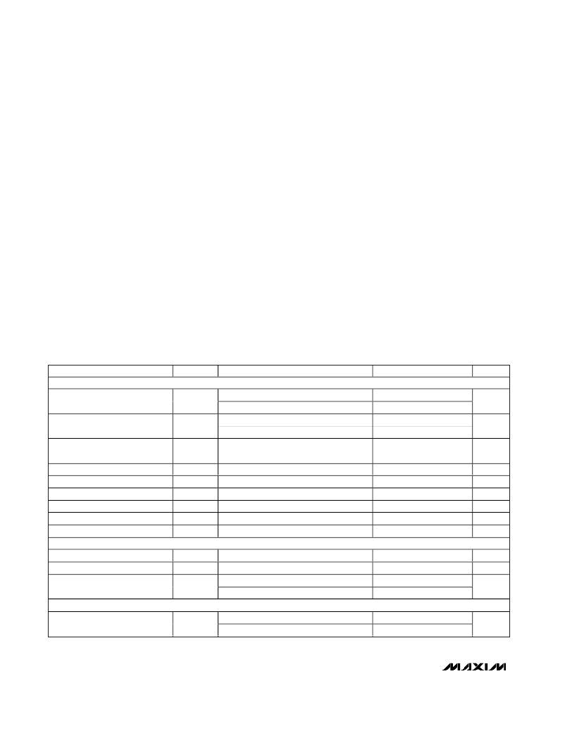
�ELECTRICAL� CHARACTERISTICS�
�(AV� DD� =� DV� DD� =� DAC_VDD� =� +2.7V� to� +5.25V,� GND� =� 0,� LEDG� =� 0,� V� LEDV� =� +2.7V� to� +5.25V,� V� REF+� -� V� REF-� =� 2.048V� (external�
�reference),� V� EXT� =� 7V,� V� REG_AMP� =� +5.0V,� C� REF+� =� 0.1μF,� REF-� =� GND,� C� NEGV� =� 0.1μF.� Internal� clock� mode,� unless� otherwise�
�noted.� All� specifications� are� at� T� A� =� T� MIN� to� T� MAX� .� Typical� values� are� at� T� A� =� +25°C,� unless� otherwise� noted.)�
�PARAMETER�
�SYMBOL�
�CONDITIONS�
�MIN�
�TYP�
�MAX�
�UNITS�
�ADC� ACCURACY�
�Noise-Free� Resolution�
�MAX1366�
�MAX1368�
�-19,999�
�-1999�
�+19,999�
�+1999�
�Counts�
�Integral� Nonlinearity� (Note� 1)�
�Range-Change� Ratio�
�Rollover� Error�
�Output� Noise�
�INL�
�2.000V� range�
�200mV� range�
�(V� AIN+� -� V� AIN-� =� 0.100V)� on� 200mV� range;�
�(V� AIN+� -� V� AIN-� =� 0.100V)� on� 2.0V� range�
�V� AIN+� -� V� AIN-� =� full� scale�
�±1�
�±1�
�10:1�
�±1�
�10�
�Counts�
�Ratio�
�Counts�
�μV� P-P�
�Offset� Error� (Zero� Input� Reading)�
�Gain� Error�
�Offset� Drift� (Zero� Reading� Drift)�
�Gain� Drift�
�V� AIN+� -� V� AIN-� =� 0� (Note� 2)�
�(Note� 3)�
�V� AIN+� -� V� AIN-� =� 0� (Note� 4)�
�-0�
�-0.5�
�0.1�
�±1�
�+0�
�+0.5�
�Counts�
�%FSR�
�μV/°C�
�ppm/°C�
�INPUT� CONVERSION� RATE�
�External� Clock� Frequency�
�4.9152�
�MHz�
�External� Clock� Duty� Cycle�
�Update� Rate�
�Internal� clock�
�External� clock,� f� CLK� =� 4.9152MHz�
�40�
�5�
�5�
�60�
�%�
�Hz�
�ANALOG� INPUTS� (AIN+,� AIN-)� (bypass� to� GND� with� 0.1μF� or� greater� capacitors)�
�AIN� Input� Voltage� Range� (Note� 5)�
�RANGE� bit� =� 0�
�RANGE� bit� =� 1�
�-2.0�
�-0.2�
�+2.0�
�+0.2�
�V�
�2�
�_______________________________________________________________________________________�
�相关PDF资料 |
PDF描述 |
|---|---|
| VI-22W-CX-F4 | CONVERTER MOD DC/DC 5.5V 75W |
| VI-22W-CX-F3 | CONVERTER MOD DC/DC 5.5V 75W |
| MAX7232BFIQH+D | IC DRVR DECODE 8DIG 44-PLCC |
| RCB92DHFT-S250 | EDGECARD PCI 184POS .050 5V SMD |
| VI-22W-CX-F2 | CONVERTER MOD DC/DC 5.5V 75W |
相关代理商/技术参数 |
参数描述 |
|---|---|
| MAX1366EVKIT | 功能描述:LED 照明开发工具 MAX1366 EVAL KIT RoHS:否 制造商:Fairchild Semiconductor 产品:Evaluation Kits 用于:FL7732 核心: 电源电压:120V 系列: 封装: |
| MAX1366EVKIT+ | 功能描述:LED 照明开发工具 MAX1366 Eval Kit RoHS:否 制造商:Fairchild Semiconductor 产品:Evaluation Kits 用于:FL7732 核心: 电源电压:120V 系列: 封装: |
| MAX1367ECM | 功能描述:LED显示驱动器 RoHS:否 制造商:Micrel 数位数量:5 片段数量: 安装风格:SMD/SMT 封装 / 箱体:PLCC-44 工作电源电压:4.75 V to 11 V 最大电源电流:10 mA 最大工作温度:+ 85 C 最小工作温度:- 40 C 封装:Tube |
| MAX1367ECM+ | 功能描述:LED显示驱动器 Stand-Alone 3.5Digit Panel Meters RoHS:否 制造商:Micrel 数位数量:5 片段数量: 安装风格:SMD/SMT 封装 / 箱体:PLCC-44 工作电源电压:4.75 V to 11 V 最大电源电流:10 mA 最大工作温度:+ 85 C 最小工作温度:- 40 C 封装:Tube |
| MAX1367ECM+T | 功能描述:LED显示驱动器 Stand-Alone 3.5Digit Panel Meters RoHS:否 制造商:Micrel 数位数量:5 片段数量: 安装风格:SMD/SMT 封装 / 箱体:PLCC-44 工作电源电压:4.75 V to 11 V 最大电源电流:10 mA 最大工作温度:+ 85 C 最小工作温度:- 40 C 封装:Tube |
发布紧急采购,3分钟左右您将得到回复。