参数资料
| 型号: | MAX1409CAP+ |
| 厂商: | Maxim Integrated Products |
| 文件页数: | 21/48页 |
| 文件大小: | 0K |
| 描述: | IC DAS 16BIT LP 20-SSOP |
| 产品培训模块: | Lead (SnPb) Finish for COTS Obsolescence Mitigation Program |
| 标准包装: | 66 |
| 类型: | 数据采集系统(DAS) |
| 分辨率(位): | 16 b |
| 采样率(每秒): | 60 |
| 数据接口: | 串行 |
| 电压电源: | 模拟和数字 |
| 电源电压: | 2.7 V ~ 3.6 V |
| 工作温度: | 0°C ~ 70°C |
| 安装类型: | 表面贴装 |
| 封装/外壳: | 20-SSOP(0.209",5.30mm 宽) |
| 供应商设备封装: | 20-SSOP |
| 包装: | 管件 |
第1页第2页第3页第4页第5页第6页第7页第8页第9页第10页第11页第12页第13页第14页第15页第16页第17页第18页第19页第20页当前第21页第22页第23页第24页第25页第26页第27页第28页第29页第30页第31页第32页第33页第34页第35页第36页第37页第38页第39页第40页第41页第42页第43页第44页第45页第46页第47页第48页
MAX1407/MAX1408/MAX1409/MAX1414
Low-Power, 16-Bit Multichannel DAS with
Internal Reference,10-Bit DACs, and RTC
28
______________________________________________________________________________________
The Offset register contains the 16-bit result from the
most recently completed ADC offset calibration. The
data format is two’s complement and is subtracted from
the filter output before writing to the Data register. After
power-up, the Offset register contains all zeros.
Each change in ambient operating condition (power
supply and temperature), PGA gain, bipolar/unipolar
input range, buffered/unbuffered mode, or conversion
speed requires an offset calibration. The offset for a
given ADC configuration can be read and stored by the
P to avoid ADC recalibration. When returning to an
ADC configuration where the offset was stored, write
back the stored offset to the Offset register. The stored
offset stays valid as long as the ambient operating con-
dition remains unchanged (within ±20°C).
Force Sense DAC Registers
(MAX1407/MAX1409/MAX1414 only)
Writing to the DAC1 register updates the output of
DAC1. Writing to the DAC2 register updates the output
of DAC2. The DAC data is 10-bit long and left justified.
Follow the timing diagrams of Figure 11 and Figure 13
to program these registers. Writing a logic 0 to the
DA1E or DA2E bit in the POWER2 register disables
DAC1 or DAC2, respectively. At power-up, DAC1 and
DAC2 are disabled.
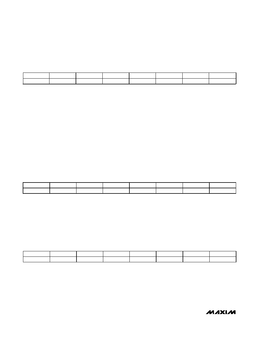
OFFSET REGISTER (00011)
FIRST BIT (MSB)
OFF15
OFF14
OFF13
OFF12
OFF11
OFF10
OFF9
OFF8
OFF7
OFF6
OFF5
OFF4
OFF3
OFF2
OFF1
OFF0
(LSB)
DAC2 REGISTER (00101)
Writing to the DAC1 register will update the DAC1 output
(OUT1). The output voltage in a unity gain configuration is
VREF x N/(2
10), where N is the integer value of DAC1[9:0]
(0 to 1023), and VREF is the reference voltage for the
DAC. The DAC1 data is 10-bit long and left justified. After
power-up, the DAC1 register contains all zeros.
FIRST BIT (MSB)
DAC1[9]
DAC1[8]
DAC1[7]
DAC1[6]
DAC1[5]
DAC1[4]
DAC1[3]
DAC1[2]
DAC1[1]
DAC1[0]
x
xxxxx
(LSB)
DAC1 REGISTER (00100)
Writing to the DAC2 register will update the DAC2 output
(OUT2). The output voltage in a unity-gain configuration is
VREF x N/(2
10), where N is the integer value of DAC2[9:0]
(0 to 1023), and VREF is the reference voltage for the
DAC. The DAC2 data is 10-bit long and left justified. After
power-up, the DAC2 register contains all zeros.
FIRST BIT (MSB)
DAC2[9]
DAC2[8]
DAC2[7]
DAC2[6]
DAC2[5]
DAC2[4]
DAC2[3]
DAC2[2]
DAC2[1]
DAC2[0]
x
xxxxx
(LSB)
相关PDF资料 |
PDF描述 |
|---|---|
| V110A28M300BL2 | CONVERTER MOD DC/DC 28V 300W |
| NBXDBA014LN1TAG | IC CLK XO 62.5/125MHZ 6CLCC |
| MS27508E16B6PA | CONN RCPT 6POS BOX MNT W/PINS |
| MS27484T20F41S | CONN PLUG 41POS STRAIGHT W/SCKT |
| V110A28M300BL | CONVERTER MOD DC/DC 28V 300W |
相关代理商/技术参数 |
参数描述 |
|---|---|
| MAX1409CAP+ | 功能描述:ADC / DAC多通道 16-Bit 60sps 1.35V Precision ADC RoHS:否 制造商:Texas Instruments 转换速率: 分辨率:8 bit 接口类型:SPI 电压参考: 电源电压-最大:3.6 V 电源电压-最小:2 V 最大工作温度:+ 85 C 安装风格:SMD/SMT 封装 / 箱体:VQFN-40 |
| MAX1409CAP+T | 功能描述:ADC / DAC多通道 16-Bit 60sps 1.35V Precision ADC RoHS:否 制造商:Texas Instruments 转换速率: 分辨率:8 bit 接口类型:SPI 电压参考: 电源电压-最大:3.6 V 电源电压-最小:2 V 最大工作温度:+ 85 C 安装风格:SMD/SMT 封装 / 箱体:VQFN-40 |
| MAX1409CAP-T | 功能描述:ADC / DAC多通道 RoHS:否 制造商:Texas Instruments 转换速率: 分辨率:8 bit 接口类型:SPI 电压参考: 电源电压-最大:3.6 V 电源电压-最小:2 V 最大工作温度:+ 85 C 安装风格:SMD/SMT 封装 / 箱体:VQFN-40 |
| MAX1409EAP | 制造商:Maxim Integrated Products 功能描述:LOW-POWER, 16-BIT MULTICHANNEL DAS WITH INTER - Bulk |
| MAX140C/D | 功能描述:模数转换器 - ADC RoHS:否 制造商:Texas Instruments 通道数量:2 结构:Sigma-Delta 转换速率:125 SPs to 8 KSPs 分辨率:24 bit 输入类型:Differential 信噪比:107 dB 接口类型:SPI 工作电源电压:1.7 V to 3.6 V, 2.7 V to 5.25 V 最大工作温度:+ 85 C 安装风格:SMD/SMT 封装 / 箱体:VQFN-32 |
发布紧急采购,3分钟左右您将得到回复。