参数资料
| 型号: | MAX1414CAI+T |
| 厂商: | Maxim Integrated Products |
| 文件页数: | 12/48页 |
| 文件大小: | 0K |
| 描述: | IC DAS 16BIT LP 28-SSOP |
| 产品培训模块: | Lead (SnPb) Finish for COTS Obsolescence Mitigation Program |
| 标准包装: | 2,000 |
| 类型: | 数据采集系统(DAS) |
| 分辨率(位): | 16 b |
| 采样率(每秒): | 60 |
| 数据接口: | 串行 |
| 电压电源: | 模拟和数字 |
| 电源电压: | 2.7 V ~ 3.6 V |
| 工作温度: | 0°C ~ 70°C |
| 安装类型: | 表面贴装 |
| 封装/外壳: | 28-SSOP(0.209",5.30mm 宽) |
| 供应商设备封装: | 28-SSOP |
| 包装: | 带卷 (TR) |
第1页第2页第3页第4页第5页第6页第7页第8页第9页第10页第11页当前第12页第13页第14页第15页第16页第17页第18页第19页第20页第21页第22页第23页第24页第25页第26页第27页第28页第29页第30页第31页第32页第33页第34页第35页第36页第37页第38页第39页第40页第41页第42页第43页第44页第45页第46页第47页第48页
MAX1407/MAX1408/MAX1409/MAX1414
Low-Power, 16-Bit Multichannel DAS with
Internal Reference,10-Bit DACs, and RTC
2
_______________________________________________________________________________________
ABSOLUTE MAXIMUM RATINGS
Stresses beyond those listed under “Absolute Maximum Ratings” may cause permanent damage to the device. These are stress ratings only, and functional
operation of the device at these or any other conditions beyond those indicated in the operational sections of the specifications is not implied. Exposure to
absolute maximum rating conditions for extended periods may affect device reliability.
AVDD to AGND .........................................................-0.3V to +6V
AVDD to DVDD ...................................................... -0.3V to +0.3V
Analog Inputs to AGND .........................-0.3V to +(AVDD + 0.3V)
Digital Inputs to DGND.............................................-0.3V to +6V
Maximum Current Input Into Any Pin ..................................50mA
Continuous Power Dissipation (TA = +70°C)
20-Pin SSOP (derate 8.0mW/°C above +70°C) ...........640mW
28-Pin SSOP (derate 9.52mW/°C above +70°C) .........762mW
DVDD to DGND.........................................................-0.3V to +6V
AGND to DGND.....................................................-0.3V to +0.3V
Analog Outputs to AGND ......................-0.3V to +(AVDD + 0.3V)
Digital Outputs to DGND .......................-0.3V to +(AVDD + 0.3V)
REF to AGND.........................................-0.3V to +(AVDD + 0.3V)
Operating Temperature Range:
MAX14__CA_ ......................................................0°C to +70°C
MAX14__EA_ ...................................................-40°C to +85°C
Lead Temperature (soldering, 10s) ................................+300 °C
Storage Temperature Range .............................-65°C to +150°C
Junction Temperature ......................................................+150°C
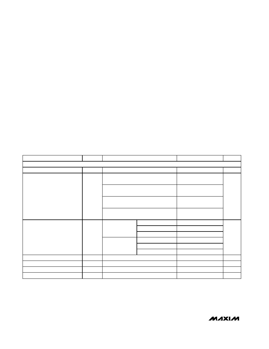
ELECTRICAL CHARACTERISTICS
(DVDD = AVDD = +2.7V to 3.6V, 4.7F at REF, internal VREF, 18nF between CPLL and AVDD, 32.768kHz crystal across CLKIN and
CLKOUT, TA = TMIN to TMAX, unless otherwise noted. Typical values are at TA = +25°C.)
PARAMETER
SYMBOL
CONDITIONS
MIN
TYP
MAX
UNITS
ADC ACCURACY
Resolution (No Missing Codes)
RES
16
Bits
Unbuffered mode, Unipolar mode, gain = 1,
VNEG = 0.2V, fully differential input (Note 7)
1.5
3.5
Unbuffered mode, Unipolar mode, gain = 2,
VNEG = 0.625V, pseudo-differential input
1.75
Unbuffered mode, Bipolar mode, gain = 1,
VNEG = 0.625V, fully differential input
1.70
Integral Nonlinearity
INL
Buffered mode, Bipolar mode, gain = 2,
VNEG = 0.625V, fully differential input
2.50
LSB
Gain = 2
±5
Gain = 1
±10
Unipolar
Gain = 1/3
±30
Gain = 2
±8
Gain = 1
±16.5
Output RMS Noise (Note 1)
Bipolar Mode
Gain = 1/3
±48.5
VRMS
Offset Error
On-chip calibration removes this error
±1
% of FSR
Offset Drift
±0.5
V/°C
Gain Error
Excludes offset and reference errors
±1
% of FSR
Gain Drift
Excludes offset and reference errors
±1
ppm/°C
相关PDF资料 |
PDF描述 |
|---|---|
| MAX1441GUP/V+ | IC PROXMITY SENSOR 2CH 20-TSSOP |
| MAX14502AETL+T | IC CARD READER USB-SD 40-TQFN |
| MAX14505EWC+T | IC SWITCH DUAL SPDT 12WLP |
| MAX14523BATA/V+T | IC CURRENT LIMIT SWITCH 8TDFN |
| MAX1452AAE+T | IC SENSOR SIGNAL COND 16-SSOP |
相关代理商/技术参数 |
参数描述 |
|---|---|
| MAX1414EAI | 制造商:Maxim Integrated Products 功能描述:LOW-POWER, 16-BIT MULTICHANNEL DAS WITH INTER - Bulk |
| MAX1414EAI+ | 制造商:Maxim Integrated Products 功能描述:LOW-POWER 16-BIT MULTICHANNEL DAS - Rail/Tube |
| MAX1414EAI+T | 制造商:Maxim Integrated Products 功能描述:LOW-POWER 16-BIT MULTICHANNEL DAS - Tape and Reel |
| MAX1415AENE | 功能描述:模数转换器 - ADC RoHS:否 制造商:Texas Instruments 通道数量:2 结构:Sigma-Delta 转换速率:125 SPs to 8 KSPs 分辨率:24 bit 输入类型:Differential 信噪比:107 dB 接口类型:SPI 工作电源电压:1.7 V to 3.6 V, 2.7 V to 5.25 V 最大工作温度:+ 85 C 安装风格:SMD/SMT 封装 / 箱体:VQFN-32 |
| MAX1415AEUE | 功能描述:模数转换器 - ADC RoHS:否 制造商:Texas Instruments 通道数量:2 结构:Sigma-Delta 转换速率:125 SPs to 8 KSPs 分辨率:24 bit 输入类型:Differential 信噪比:107 dB 接口类型:SPI 工作电源电压:1.7 V to 3.6 V, 2.7 V to 5.25 V 最大工作温度:+ 85 C 安装风格:SMD/SMT 封装 / 箱体:VQFN-32 |
发布紧急采购,3分钟左右您将得到回复。