- 您现在的位置:买卖IC网 > PDF目录10566 > MAX1416EUE+ (Maxim Integrated Products)IC ADC 16BIT DELTA SIGMA 16TSSOP PDF资料下载
参数资料
| 型号: | MAX1416EUE+ |
| 厂商: | Maxim Integrated Products |
| 文件页数: | 19/36页 |
| 文件大小: | 0K |
| 描述: | IC ADC 16BIT DELTA SIGMA 16TSSOP |
| 产品培训模块: | MAX11200 ADC Lead (SnPb) Finish for COTS Obsolescence Mitigation Program |
| 标准包装: | 96 |
| 位数: | 16 |
| 采样率(每秒): | 500 |
| 数据接口: | MICROWIRE?,QSPI?,串行,SPI? |
| 转换器数目: | 1 |
| 功率耗散(最大): | 755mW |
| 电压电源: | 单电源 |
| 工作温度: | -45°C ~ 85°C |
| 安装类型: | 表面贴装 |
| 封装/外壳: | 16-TSSOP(0.173",4.40mm 宽) |
| 供应商设备封装: | 16-TSSOP |
| 包装: | 管件 |
| 输入数目和类型: | 2 个差分,单极;2 个差分,双极 |
第1页第2页第3页第4页第5页第6页第7页第8页第9页第10页第11页第12页第13页第14页第15页第16页第17页第18页当前第19页第20页第21页第22页第23页第24页第25页第26页第27页第28页第29页第30页第31页第32页第33页第34页第35页第36页
MAX1415/MAX1416
Clock Register
The byte-wide clock register is bidirectional, so it can
be written and read. The byte written to the setup regis-
ter sets the clock, filter first notch frequency, and the
output data rate (see Table 12).
MXID: (Default = 1) Maxim-Identifier Bit. This is a read-
only bit. Values written to this bit are ignored.
ZERO: (Default = 0) Zero Bit. This is a read-only bit.
Values written to this bit are ignored.
INTCLK: (Default = 0) Internal Oscillator Bit. Set INTCLK
= 1 to enable the internal oscillator. Set INTCLK = 0 to
disable the internal oscillator.
CLKDIS: (Default = 0) Clock-Disable Bit. Set CLKDIS = 1
to disable the internally or externally generated clock from
appearing on CLKOUT. When using a crystal or res-
onator across CLKIN and CLKOUT, the clock is stopped
and no conversions take place when CLKDIS = 1.
CLKOUT is held low during clock disable to save power.
Set CLKDIS = 0 to allow other devices to use the output
signal on CLKOUT as a clock source and/or to enable the
external oscillator. The CLKOUT pin on the MAX1415/
MAX1416 can drive one CMOS load.
CLKDIV: (Default = 0) Clock-Divider Control Bit. The
MAX1415/MAX1416 each have an internal clock divider.
Set this bit to 1 to divide the input clock by two. When this
bit is set to 0, the MAX1415/MAX1416 operate at the
internal or external oscillator frequency. CLKDIV has no
effect on the internal oscillator.
CLK: (Default = 1) Clock Bit. When using the internal
oscillator (INTCLK = 1), set CLK = 1 for a frequency of
2.4576MHz, and set CLK = 0 for a frequency of 1MHz.
When using an external clock/oscillator, set CLK = 1 for
fCLKIN = 2.4576MHz with CLKDIV = 0, or fCLKIN =
4.9152MHz with CLKDIV = 1.
16-Bit, Low-Power, 2-Channel,
Sigma-Delta ADCs
26
______________________________________________________________________________________
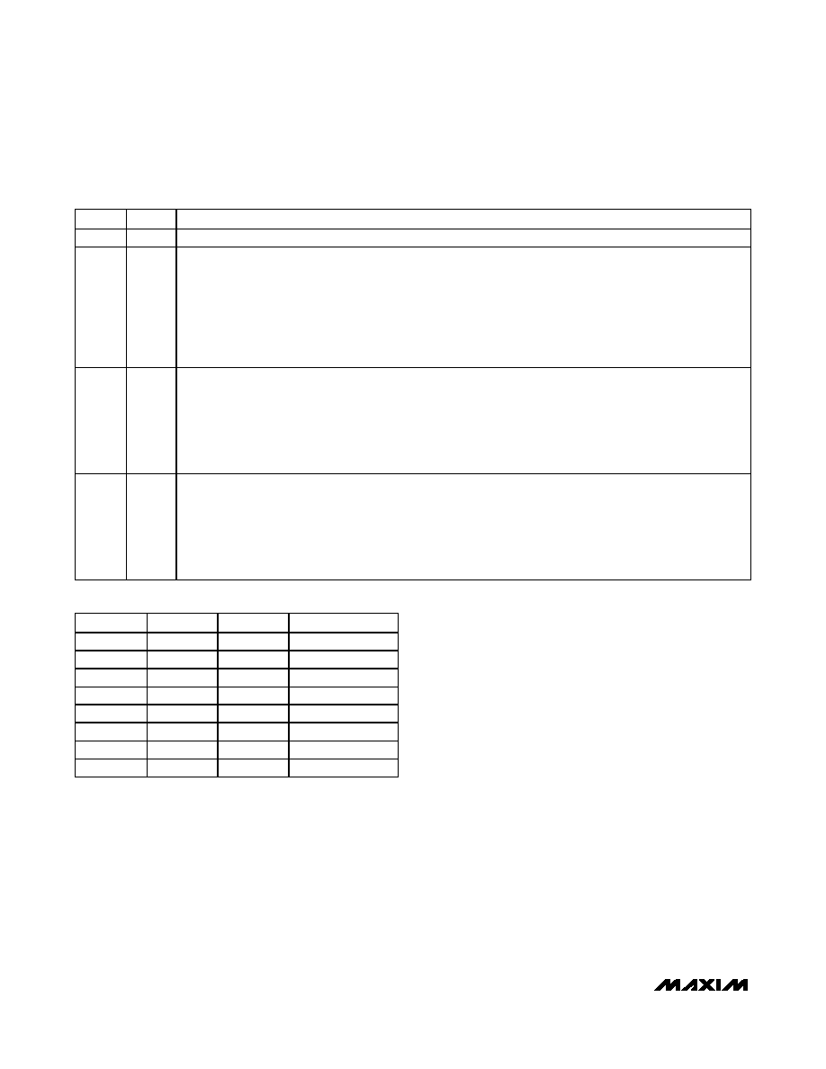
Table 10. Operating-Mode Selection
MD1
MD0
OPERATING MODE
0
Normal Mode. Use this mode to perform normal conversions on the selected analog input channel.
01
Self-Calibration Mode. This mode performs self-calibration on the selected channel determined from CH0 and
CH1 selection bits in the communications register (Table 6). Upon completion of self-calibration, the device
returns to normal mode with MD1, MD0 returning to 0, 0. The
DRDY output bit goes high when self-calibration is
requested and returns low when the calibration is complete and a new data word is in the data register. Self-
calibration performs an internal zero-scale and full-scale calibration. The analog inputs of the device are shorted
together internally during zero-scale calibration and connected to an internally generated (VREF/GAIN) voltage
during full-scale calibration. The offset and gain registers for the selected channel are automatically updated
with the calibration data.
10
Zero-Scale System-Calibration Mode. This mode performs zero-scale calibration on the selected channel
determined from CH1 and CH0 selection bits in the communications register (Table 6). The
DRDY output bit
goes high when calibration is requested and returns low when the calibration is complete and a new data word
is in the data register. Performing zero-scale calibration compensates for any DC offset voltage present in the
ADC and system. Ensure that the analog input voltage is stable within 0.5 LSB for the duration of the calibration
sequence. The offset register for the selected channel is updated with the zero-scale system-calibration data.
Upon completion of calibration, the device returns to normal mode with MD1, MD0 returning to 0, 0.
11
Full-Scale System-Calibration Mode. This mode performs full-scale system-calibration on the selected channel
determined from CH1 and CH0 selection bits in the communications register. This calibration assigns a full-
scale output code to the voltage present on the selected channel. Ensure that the analog input voltage is stable
within 0.5 LSB for the duration of the calibration sequence. The
DRDY output bit goes high during calibration
and returns low when the calibration is complete and a new data word is in the data register. The gain register
for the selected channel is updated with the full-scale system-calibration data. Upon completion of calibration,
the device returns to normal mode with MD1, MD0 returning to 0, 0.
Table 11. PGA Gain Selection
G2
G1
G0
PGA GAIN
00
0
1
00
1
2
01
0
4
01
1
8
10
0
16
10
1
32
11
0
64
1
128
相关PDF资料 |
PDF描述 |
|---|---|
| AD7942BCPZRL7 | IC ADC 14BIT 250KSPS 10-LFCSP |
| VE-251-IW-F4 | CONVERTER MOD DC/DC 12V 100W |
| VI-25X-MX | CONVERTER MOD DC/DC 5.2V 75W |
| VE-251-IW-F2 | CONVERTER MOD DC/DC 12V 100W |
| VE-251-IW-F1 | CONVERTER MOD DC/DC 12V 100W |
相关代理商/技术参数 |
参数描述 |
|---|---|
| MAX1416EUE+ | 功能描述:模数转换器 - ADC 16-Bit 2Ch .5ksps 3.5V Precision ADC RoHS:否 制造商:Texas Instruments 通道数量:2 结构:Sigma-Delta 转换速率:125 SPs to 8 KSPs 分辨率:24 bit 输入类型:Differential 信噪比:107 dB 接口类型:SPI 工作电源电压:1.7 V to 3.6 V, 2.7 V to 5.25 V 最大工作温度:+ 85 C 安装风格:SMD/SMT 封装 / 箱体:VQFN-32 |
| MAX1416EUE+T | 功能描述:模数转换器 - ADC 16-Bit 2Ch .5ksps 3.5V Precision ADC RoHS:否 制造商:Texas Instruments 通道数量:2 结构:Sigma-Delta 转换速率:125 SPs to 8 KSPs 分辨率:24 bit 输入类型:Differential 信噪比:107 dB 接口类型:SPI 工作电源电压:1.7 V to 3.6 V, 2.7 V to 5.25 V 最大工作温度:+ 85 C 安装风格:SMD/SMT 封装 / 箱体:VQFN-32 |
| MAX1416EUE-T | 功能描述:模数转换器 - ADC RoHS:否 制造商:Texas Instruments 通道数量:2 结构:Sigma-Delta 转换速率:125 SPs to 8 KSPs 分辨率:24 bit 输入类型:Differential 信噪比:107 dB 接口类型:SPI 工作电源电压:1.7 V to 3.6 V, 2.7 V to 5.25 V 最大工作温度:+ 85 C 安装风格:SMD/SMT 封装 / 箱体:VQFN-32 |
| MAX1416EVC16 | 功能描述:模数转换器 - ADC MAX1416 Evaluation Kit/Evaluation System RoHS:否 制造商:Texas Instruments 通道数量:2 结构:Sigma-Delta 转换速率:125 SPs to 8 KSPs 分辨率:24 bit 输入类型:Differential 信噪比:107 dB 接口类型:SPI 工作电源电压:1.7 V to 3.6 V, 2.7 V to 5.25 V 最大工作温度:+ 85 C 安装风格:SMD/SMT 封装 / 箱体:VQFN-32 |
| MAX1416EVKIT | 功能描述:数据转换 IC 开发工具 MAX1416 Evaluation Kit/Evaluation System RoHS:否 制造商:Texas Instruments 产品:Demonstration Kits 类型:ADC 工具用于评估:ADS130E08 接口类型:SPI 工作电源电压:- 6 V to + 6 V |
发布紧急采购,3分钟左右您将得到回复。