- 您现在的位置:买卖IC网 > PDF目录9956 > MAX1416EUE+T (Maxim Integrated Products)IC ADC 16BIT DELTA SIGMA 16TSSOP PDF资料下载
参数资料
| 型号: | MAX1416EUE+T |
| 厂商: | Maxim Integrated Products |
| 文件页数: | 26/36页 |
| 文件大小: | 0K |
| 描述: | IC ADC 16BIT DELTA SIGMA 16TSSOP |
| 产品培训模块: | Lead (SnPb) Finish for COTS Obsolescence Mitigation Program |
| 标准包装: | 2,500 |
| 位数: | 16 |
| 采样率(每秒): | 500 |
| 数据接口: | MICROWIRE?,QSPI?,串行,SPI? |
| 转换器数目: | 1 |
| 功率耗散(最大): | 755mW |
| 电压电源: | 单电源 |
| 工作温度: | -45°C ~ 85°C |
| 安装类型: | 表面贴装 |
| 封装/外壳: | 16-TSSOP(0.173",4.40mm 宽) |
| 供应商设备封装: | 16-TSSOP |
| 包装: | 带卷 (TR) |
| 输入数目和类型: | 2 个差分,单极;2 个差分,双极 |
第1页第2页第3页第4页第5页第6页第7页第8页第9页第10页第11页第12页第13页第14页第15页第16页第17页第18页第19页第20页第21页第22页第23页第24页第25页当前第26页第27页第28页第29页第30页第31页第32页第33页第34页第35页第36页
MAX1415/MAX1416
Applications Information
Applications Examples
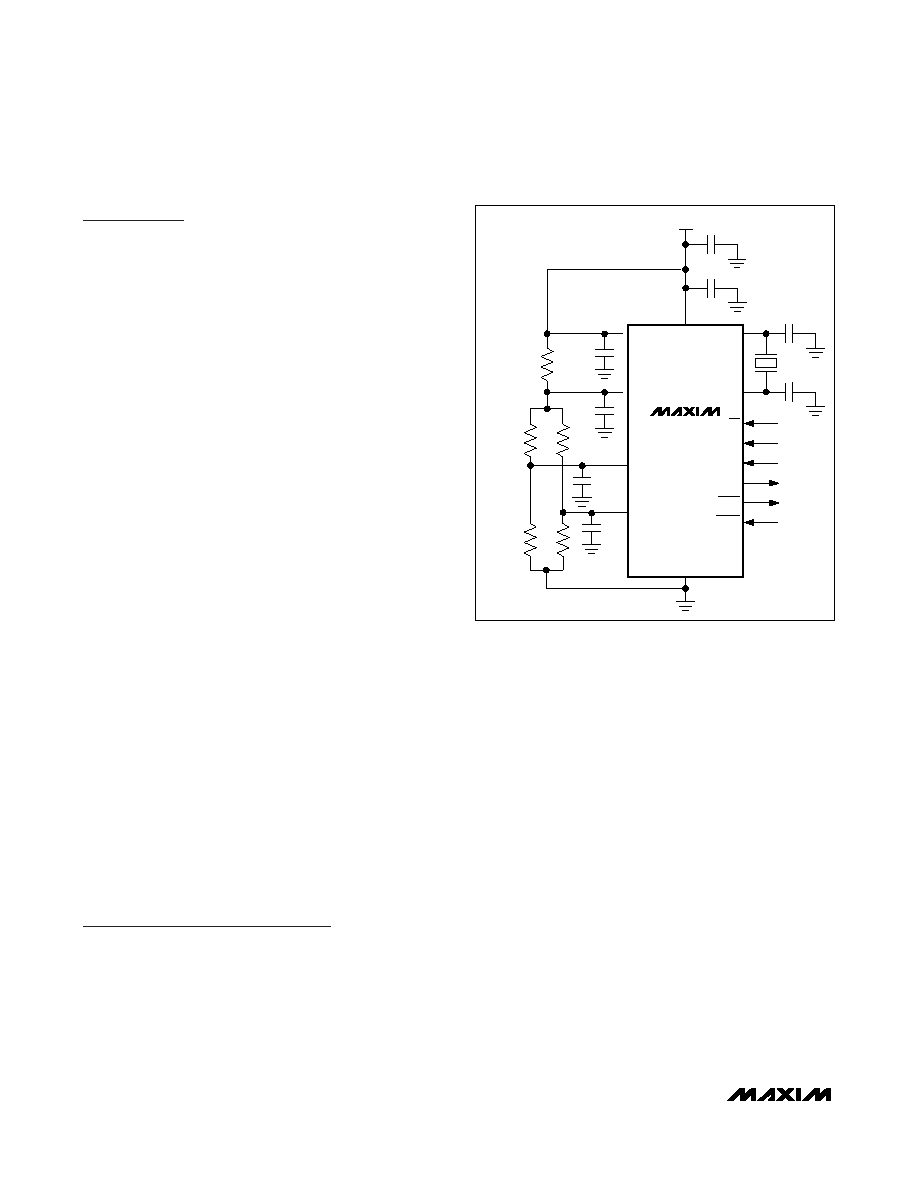
Strain-Gauge Measurement
Connect the differential inputs of the MAX1415/
MAX1416 to the bridge network of the strain gauge. In
Figure 12, the analog positive supply voltage powers the
bridge network and the MAX1415/MAX1416 along with
the reference voltage in a ratiometric configuration. The
on-chip PGA allows the MAX1415/MAX1416 to handle an
analog input voltage range as low as 20mV to full scale.
Optical Isolation
For applications that require an optically isolated inter-
face, see Figure 13. With 6N136-type optocouplers, the
maximum clock speed is 4MHz. The maximum clock
speed is limited by the degree of mismatch between
the individual optocouplers. Faster optocouplers allow
faster signaling at a higher cost.
Layout, Grounding, and Bypassing
Use PC boards with separate analog and digital
ground planes. Connect the two ground planes togeth-
er at the MAX1415/MAX1416 GND. Isolate the digital
supply from the analog with a low-value resistor (10
)
or ferrite bead when the analog and digital supplies
come from the same source.
Ensure that digital return currents do not pass through
the analog ground and that return-current paths are low
impedance. A 5mA current flowing through a PC board
ground trace impedance of only 0.05
creates an error
voltage of approximately 250V.
Layout the PC board to ensure digital and analog signal
lines are kept separate. Do not run digital lines (especial-
ly the SCLK and DOUT) parallel to any analog lines. If
they must cross one another, do so at right angles.
Bypass VDD to the analog ground plane with a 0.1F
capacitor in parallel with a 1F to 10F low-ESR capac-
itor. Keep capacitor leads short for best supply-noise
rejection. Bypass REF+, REF-, and all analog inputs
with a 0.1F capacitor to GND. Place all bypass capac-
itors as close to the device as possible to achieve the
best decoupling.
Definitions
Integral Nonlinearity
Integral nonlinearity (INL) is the deviation of the values
on an actual transfer function from a straight line. This
straight line is either a best-straight-line fit or a line
drawn between the endpoints of the transfer function,
once offset and gain errors have been nullified. INL for
the MAX1415/MAX1416 is measured using the end-
point method. This is the more conservative method.
Unipolar Offset Error
For an ideal converter, the first transition occurs at 0.5
LSB above zero. Offset error is the amount of deviation
between the measured first transition point and the
ideal point.
Bipolar Zero Error
In bipolar mode, the ideal midscale transition occurs at
AIN+ - AIN- = 0. Bipolar zero error is the measured
deviation from this ideal value.
Gain Error
With a full-scale analog input voltage applied to the
ADC (resulting in all ones in the digital code), gain error
is defined as the amount of deviation between the ideal
transfer function and the measured transfer function
(with the offset error or bipolar zero error removed).
Gain error is usually expressed in LSB or a percent of
full-scale range (%FSR).
Positive Full-Scale Error
For the ideal transfer curve, the code edge transition
that causes a full-scale transition to occur is 1.5 LSB
below full scale. The positive full-scale error is the dif-
ference between this code transition of the ideal trans-
16-Bit, Low-Power, 2-Channel,
Sigma-Delta ADCs
32
______________________________________________________________________________________
MAX1415
MAX1416
VDD
CLKIN
REF+
REF-
AIN1+
AIN1-
CLKOUT
CS
SCLK
DIN
DOUT
DRDY
RESET
GND
VDD
RREF
ACTIVE
GAUGE
DUMMY
GAUGE
0.1
F
10
F
0.1
F
0.1
F
R
0.1
F
0.1
F
Figure 12. Strain Gauge Measurement
相关PDF资料 |
PDF描述 |
|---|---|
| MS27508E16B26SB | CONN RCPT 26POS BOX MNT W/SCKT |
| IDT7208L25JI | IC FIFO 64KX9 25NS 32PLCC |
| V72B24M250BG2 | CONVERTER MOD DC/DC 24V 250W |
| V72B15M250BG3 | CONVERTER MOD DC/DC 15V 250W |
| IDT7208L25JGI | IC FIFO 64KX9 25NS 32PLCC |
相关代理商/技术参数 |
参数描述 |
|---|---|
| MAX1416EVC16 | 功能描述:模数转换器 - ADC MAX1416 Evaluation Kit/Evaluation System RoHS:否 制造商:Texas Instruments 通道数量:2 结构:Sigma-Delta 转换速率:125 SPs to 8 KSPs 分辨率:24 bit 输入类型:Differential 信噪比:107 dB 接口类型:SPI 工作电源电压:1.7 V to 3.6 V, 2.7 V to 5.25 V 最大工作温度:+ 85 C 安装风格:SMD/SMT 封装 / 箱体:VQFN-32 |
| MAX1416EVKIT | 功能描述:数据转换 IC 开发工具 MAX1416 Evaluation Kit/Evaluation System RoHS:否 制造商:Texas Instruments 产品:Demonstration Kits 类型:ADC 工具用于评估:ADS130E08 接口类型:SPI 工作电源电压:- 6 V to + 6 V |
| MAX1416EWE | 功能描述:模数转换器 - ADC RoHS:否 制造商:Texas Instruments 通道数量:2 结构:Sigma-Delta 转换速率:125 SPs to 8 KSPs 分辨率:24 bit 输入类型:Differential 信噪比:107 dB 接口类型:SPI 工作电源电压:1.7 V to 3.6 V, 2.7 V to 5.25 V 最大工作温度:+ 85 C 安装风格:SMD/SMT 封装 / 箱体:VQFN-32 |
| MAX1416EWE+ | 功能描述:模数转换器 - ADC 16-Bit 2Ch .5ksps 3.5V Precision ADC RoHS:否 制造商:Texas Instruments 通道数量:2 结构:Sigma-Delta 转换速率:125 SPs to 8 KSPs 分辨率:24 bit 输入类型:Differential 信噪比:107 dB 接口类型:SPI 工作电源电压:1.7 V to 3.6 V, 2.7 V to 5.25 V 最大工作温度:+ 85 C 安装风格:SMD/SMT 封装 / 箱体:VQFN-32 |
| MAX1416EWE+T | 功能描述:模数转换器 - ADC 16-Bit 2Ch .5ksps 3.5V Precision ADC RoHS:否 制造商:Texas Instruments 通道数量:2 结构:Sigma-Delta 转换速率:125 SPs to 8 KSPs 分辨率:24 bit 输入类型:Differential 信噪比:107 dB 接口类型:SPI 工作电源电压:1.7 V to 3.6 V, 2.7 V to 5.25 V 最大工作温度:+ 85 C 安装风格:SMD/SMT 封装 / 箱体:VQFN-32 |
发布紧急采购,3分钟左右您将得到回复。