- 您现在的位置:买卖IC网 > PDF目录9956 > MAX1416EUE+T (Maxim Integrated Products)IC ADC 16BIT DELTA SIGMA 16TSSOP PDF资料下载
参数资料
| 型号: | MAX1416EUE+T |
| 厂商: | Maxim Integrated Products |
| 文件页数: | 36/36页 |
| 文件大小: | 0K |
| 描述: | IC ADC 16BIT DELTA SIGMA 16TSSOP |
| 产品培训模块: | Lead (SnPb) Finish for COTS Obsolescence Mitigation Program |
| 标准包装: | 2,500 |
| 位数: | 16 |
| 采样率(每秒): | 500 |
| 数据接口: | MICROWIRE?,QSPI?,串行,SPI? |
| 转换器数目: | 1 |
| 功率耗散(最大): | 755mW |
| 电压电源: | 单电源 |
| 工作温度: | -45°C ~ 85°C |
| 安装类型: | 表面贴装 |
| 封装/外壳: | 16-TSSOP(0.173",4.40mm 宽) |
| 供应商设备封装: | 16-TSSOP |
| 包装: | 带卷 (TR) |
| 输入数目和类型: | 2 个差分,单极;2 个差分,双极 |
第1页第2页第3页第4页第5页第6页第7页第8页第9页第10页第11页第12页第13页第14页第15页第16页第17页第18页第19页第20页第21页第22页第23页第24页第25页第26页第27页第28页第29页第30页第31页第32页第33页第34页第35页当前第36页
MAX1415/MAX1416
16-Bit, Low-Power, 2-Channel,
Sigma-Delta ADCs
_______________________________________________________________________________________
9
Note 1: These errors are in the order of the conversion noise shown in Tables 1 and 3. This applies after calibration at the given
temperature.
Note 2: Recalibration at any temperature removes these drift errors.
Note 3: Positive full-scale error includes zero-scale errors (unipolar offset error or bipolar zero error) and applies to both unipolar
and bipolar input ranges.
Note 4: Full-scale drift includes zero-scale drift (unipolar offset drift or bipolar zero drift) and applies to both unipolar and bipolar
input ranges.
Note 5: Gain error does not include zero-scale errors. It is calculated as (full-scale error – unipolar offset error) for unipolar ranges,
and (full-scale error – bipolar zero error) for bipolar ranges.
Note 6: Gain-error drift does not include unipolar offset drift or bipolar zero drift. Effectively, it is the drift of the part if only zero-
scale calibrations are performed.
Note 7: The analog input voltage range on AIN+ is given here with respect to the voltage on AIN- on the MAX1415/MAX1416.
Note 8: This common-mode voltage range is allowed, provided that the input voltage on the analog inputs does not go more posi-
tive than (VDD + 30mV) or more negative than (GND - 30mV). Parts are functional with voltages down to (GND - 200mV),
but with increased leakage at high temperature.
Note 9: The REF differential voltage, VREF, is the voltage on REF+ referenced to REF- (VREF = VREF+ - VREF-).
Note 10: Guaranteed by design.
Note 11: These calibration and span limits apply, provided that the absolute voltage on the analog inputs does not exceed (VDD +
30mV) or go more negative than (GND - 30mV). The offset-calibration limit applies to both the unipolar zero point and the
bipolar zero point.
Note 12: When using a crystal or ceramic resonator across the CLKIN and CLKOUT as the clock source for the device, the supply
current and power dissipation varies depending on the crystal or resonator type. Supply current is measured with the digi-
tal inputs connected to 0 or VDD, CLKIN connected to an external clock source, and CLKDIS = 1.
Note 13: If the external master clock continues to run in power-down mode, the power-down current typically increases to 67A at
3V. When using a crystal or ceramic resonator across the CLKIN and CLKOUT as the clock source for the device, the
clock generator continues to run in power-down mode and the power dissipation depends on the crystal or resonator type
(see the Power-Down Modes section).
Note 14: Measured at DC and applied in the selected passband. PSRR at 50Hz exceeds 120dB with filter notches of 25Hz or 50Hz.
PSRR at 60Hz exceeds 120dB with filter notches of 20Hz or 60Hz.
PSRR depends on both gain and VDD.
Note 15: Provide fCLKIN whenever the MAX1415/MAX1416 are not in power-down mode. If no clock is present, the device can draw
higher-than-specified current and can possibly become uncalibrated.
Note 16: All input signals are specified with tr = tf = 5ns (10% to 90% of VDD) and timed from a voltage level of 1.6V.
GAIN
PSRR (VDD = 5V)
PSRR (VDD = 3V)
(dB)
190
86
278
78
484
85
8 to 128
91
93
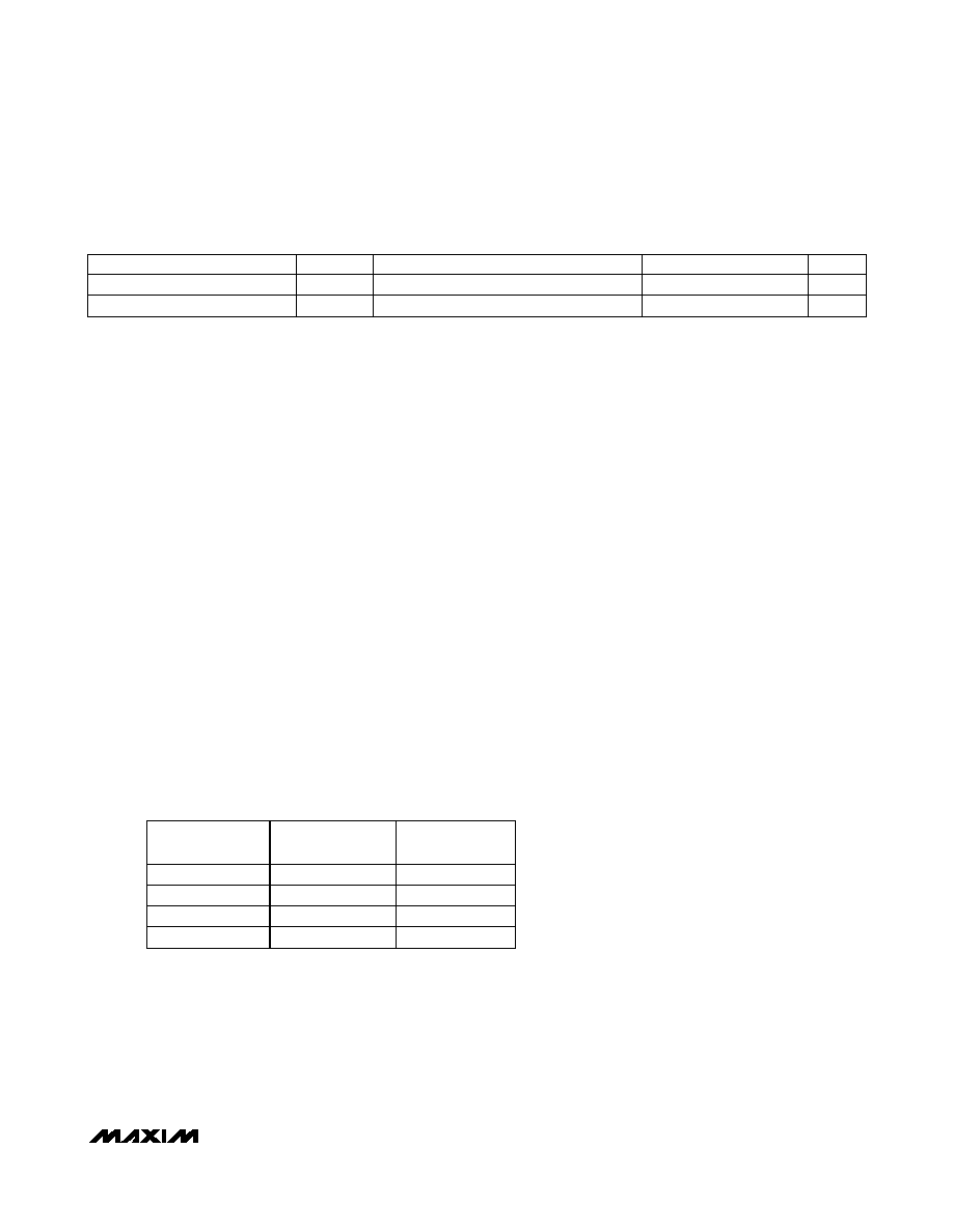
TIMING CHARACTERISTICS—MAX1416 (continued)
(Note 16) (Figures 8, 9)
PARAMETER
SYMBOL
CONDITIONS
MIN
TYP
MAX
UNITS
DIN to SCLK Setup Time
t9
30
ns
DIN to SCLK Hold Time
t10
20
ns
相关PDF资料 |
PDF描述 |
|---|---|
| MS27508E16B26SB | CONN RCPT 26POS BOX MNT W/SCKT |
| IDT7208L25JI | IC FIFO 64KX9 25NS 32PLCC |
| V72B24M250BG2 | CONVERTER MOD DC/DC 24V 250W |
| V72B15M250BG3 | CONVERTER MOD DC/DC 15V 250W |
| IDT7208L25JGI | IC FIFO 64KX9 25NS 32PLCC |
相关代理商/技术参数 |
参数描述 |
|---|---|
| MAX1416EVC16 | 功能描述:模数转换器 - ADC MAX1416 Evaluation Kit/Evaluation System RoHS:否 制造商:Texas Instruments 通道数量:2 结构:Sigma-Delta 转换速率:125 SPs to 8 KSPs 分辨率:24 bit 输入类型:Differential 信噪比:107 dB 接口类型:SPI 工作电源电压:1.7 V to 3.6 V, 2.7 V to 5.25 V 最大工作温度:+ 85 C 安装风格:SMD/SMT 封装 / 箱体:VQFN-32 |
| MAX1416EVKIT | 功能描述:数据转换 IC 开发工具 MAX1416 Evaluation Kit/Evaluation System RoHS:否 制造商:Texas Instruments 产品:Demonstration Kits 类型:ADC 工具用于评估:ADS130E08 接口类型:SPI 工作电源电压:- 6 V to + 6 V |
| MAX1416EWE | 功能描述:模数转换器 - ADC RoHS:否 制造商:Texas Instruments 通道数量:2 结构:Sigma-Delta 转换速率:125 SPs to 8 KSPs 分辨率:24 bit 输入类型:Differential 信噪比:107 dB 接口类型:SPI 工作电源电压:1.7 V to 3.6 V, 2.7 V to 5.25 V 最大工作温度:+ 85 C 安装风格:SMD/SMT 封装 / 箱体:VQFN-32 |
| MAX1416EWE+ | 功能描述:模数转换器 - ADC 16-Bit 2Ch .5ksps 3.5V Precision ADC RoHS:否 制造商:Texas Instruments 通道数量:2 结构:Sigma-Delta 转换速率:125 SPs to 8 KSPs 分辨率:24 bit 输入类型:Differential 信噪比:107 dB 接口类型:SPI 工作电源电压:1.7 V to 3.6 V, 2.7 V to 5.25 V 最大工作温度:+ 85 C 安装风格:SMD/SMT 封装 / 箱体:VQFN-32 |
| MAX1416EWE+T | 功能描述:模数转换器 - ADC 16-Bit 2Ch .5ksps 3.5V Precision ADC RoHS:否 制造商:Texas Instruments 通道数量:2 结构:Sigma-Delta 转换速率:125 SPs to 8 KSPs 分辨率:24 bit 输入类型:Differential 信噪比:107 dB 接口类型:SPI 工作电源电压:1.7 V to 3.6 V, 2.7 V to 5.25 V 最大工作温度:+ 85 C 安装风格:SMD/SMT 封装 / 箱体:VQFN-32 |
发布紧急采购,3分钟左右您将得到回复。