- 您现在的位置:买卖IC网 > PDF目录9948 > MAX1422CCM+TD (Maxim Integrated Products)IC ADC 12BIT 20MSPS 48LQFP PDF资料下载
参数资料
| 型号: | MAX1422CCM+TD |
| 厂商: | Maxim Integrated Products |
| 文件页数: | 2/15页 |
| 文件大小: | 0K |
| 描述: | IC ADC 12BIT 20MSPS 48LQFP |
| 产品培训模块: | Lead (SnPb) Finish for COTS Obsolescence Mitigation Program |
| 标准包装: | 2,000 |
| 位数: | 12 |
| 采样率(每秒): | 20M |
| 数据接口: | 并联 |
| 转换器数目: | 1 |
| 功率耗散(最大): | 152mW |
| 电压电源: | 模拟和数字 |
| 工作温度: | 0°C ~ 70°C |
| 安装类型: | 表面贴装 |
| 封装/外壳: | 48-LQFP |
| 供应商设备封装: | 48-LQFP(7x7) |
| 包装: | 带卷 (TR) |
| 输入数目和类型: | 1 个差分,双极 |
MAX1422
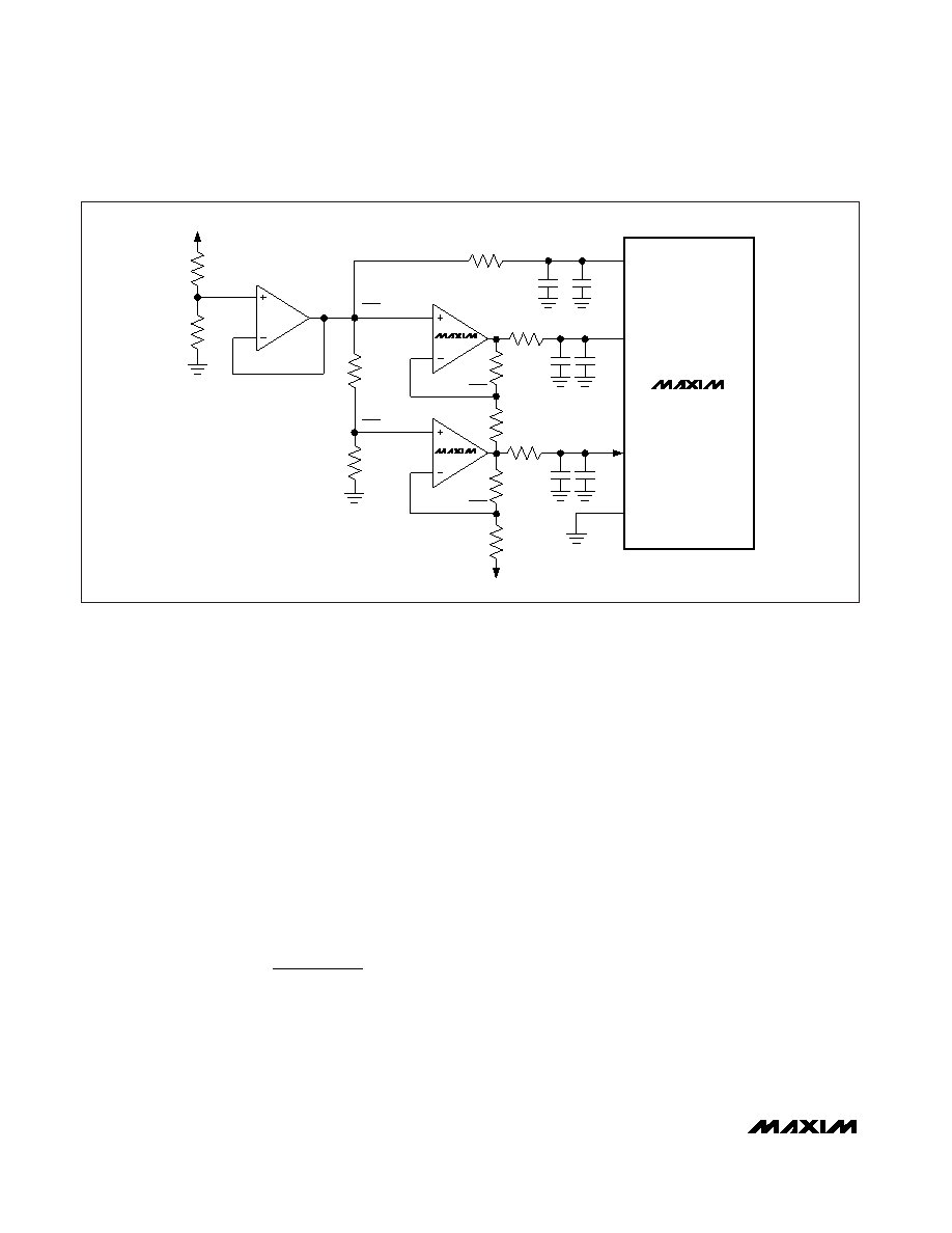
these nodes become high impedance and can be driven
by external reference sources, as shown in Figure 3.
Clock Inputs (CLK,
CLK)
The MAX1422’s CLK and CLK inputs accept both sin-
gle-ended and differential input operation, and accept
CMOS-compatible clock signals. If CLK is driven with a
single-ended clock signal, bypass CLK with a 0.1F
capacitor to AGND. Since the interstage conversion of
the device depends on the repeatability of the rising
and falling edges of the external clock, use a clock with
low jitter and fast rise and fall times (<2ns). In particu-
lar, sampling occurs on the rising edge of the clock sig-
nal, requiring this edge to have the lowest possible
jitter. Any significant aperture jitter would limit the SNR
performance of the ADC according to the following
relationship:
where fIN represents the analog input frequency, and
tAJ is the aperture jitter.
Clock jitter is especially critical for high input frequency
applications. The clock input should always be consid-
ered as an analog input and routed away from any ana-
log or digital signal lines.
The MAX1422 clock input operates with a voltage
threshold set to AVDD/2. Clock inputs must meet the
specifications for high and low periods, as stated in the
Electrical Characteristics.
Figure 4 shows a simplified model of the clock input cir-
cuit. This circuit consists of two 10k
resistors to bias
the common-mode level of each input. This circuit may
be used to AC-couple the system clock signal to the
MAX1422 clock input.
Output Enable (
OE), Power-Down (PD) and
Output Data (D0–D11)
With OE high, the digital outputs enter a high-imped-
ance state. If OE is held low with PD high, the outputs
are latched at the last value prior to the power-down.
All data outputs, D0 (LSB) through D11 (MSB), are
TTL/CMOS logic compatible. There is a seven clock-
cycle latency between any particular sample and its
valid output data. The output coding is in offset binary
format (Table 1).
The capacitive load on the digital outputs D0 through
D11 should be kept as low as possible (
≤10pF) to avoid
large digital currents that could feed back into the ana-
SNR
t
dB
IN
AJ
=×
× ×
20
1
2
10
log
π
12-Bit, 20Msps, 3.3V, Low-Power ADC with
Internal Reference
10
______________________________________________________________________________________
MAX1422
REFIN
REFN
R
50
R
1V
R
50
50
R
AVDD
CML
0.1nF
0.22
F
0.1nF
0.22
F
0.1nF
0.22
F
AGND
AVDD
4
MAX4284
REFP
AVDD
2
AVDD
4
AVDD
2
Figure 3. Unbuffered External Reference Drive—Internal Reference Disabled
相关PDF资料 |
PDF描述 |
|---|---|
| IDT72275L15PFI8 | IC FIFO 32768X18 LP 15NS 64-TQFP |
| GTC06AF-14S-5P | CONN PLUG 5POS STRAIGHT W/PINS |
| MAX148ACAP+T | IC ADC 10BIT SERIAL 20-SSOP |
| IDT72275L10PF8 | IC FIFO 32768X18 LP 10NS 64-TQFP |
| V150B24M250BF3 | CONVERTER MOD DC/DC 24V 250W |
相关代理商/技术参数 |
参数描述 |
|---|---|
| MAX1422ECM | 制造商:Maxim Integrated Products 功能描述:48 PINS TQFP PKG - Bulk |
| MAX1422ECM+D | 功能描述:模数转换器 - ADC RoHS:否 制造商:Texas Instruments 通道数量:2 结构:Sigma-Delta 转换速率:125 SPs to 8 KSPs 分辨率:24 bit 输入类型:Differential 信噪比:107 dB 接口类型:SPI 工作电源电压:1.7 V to 3.6 V, 2.7 V to 5.25 V 最大工作温度:+ 85 C 安装风格:SMD/SMT 封装 / 箱体:VQFN-32 |
| MAX1422ECM+TD | 功能描述:模数转换器 - ADC RoHS:否 制造商:Texas Instruments 通道数量:2 结构:Sigma-Delta 转换速率:125 SPs to 8 KSPs 分辨率:24 bit 输入类型:Differential 信噪比:107 dB 接口类型:SPI 工作电源电压:1.7 V to 3.6 V, 2.7 V to 5.25 V 最大工作温度:+ 85 C 安装风格:SMD/SMT 封装 / 箱体:VQFN-32 |
| MAX1422ECM-D | 功能描述:模数转换器 - ADC RoHS:否 制造商:Texas Instruments 通道数量:2 结构:Sigma-Delta 转换速率:125 SPs to 8 KSPs 分辨率:24 bit 输入类型:Differential 信噪比:107 dB 接口类型:SPI 工作电源电压:1.7 V to 3.6 V, 2.7 V to 5.25 V 最大工作温度:+ 85 C 安装风格:SMD/SMT 封装 / 箱体:VQFN-32 |
| MAX1422ECM-TD | 功能描述:模数转换器 - ADC RoHS:否 制造商:Texas Instruments 通道数量:2 结构:Sigma-Delta 转换速率:125 SPs to 8 KSPs 分辨率:24 bit 输入类型:Differential 信噪比:107 dB 接口类型:SPI 工作电源电压:1.7 V to 3.6 V, 2.7 V to 5.25 V 最大工作温度:+ 85 C 安装风格:SMD/SMT 封装 / 箱体:VQFN-32 |
发布紧急采购,3分钟左右您将得到回复。