- 您现在的位置:买卖IC网 > PDF目录17006 > MAX147EVC16-DIP (Maxim Integrated Products)EVAL KIT FOR MAX147 PDF资料下载
参数资料
| 型号: | MAX147EVC16-DIP |
| 厂商: | Maxim Integrated Products |
| 文件页数: | 7/24页 |
| 文件大小: | 0K |
| 描述: | EVAL KIT FOR MAX147 |
| 产品培训模块: | Lead (SnPb) Finish for COTS Obsolescence Mitigation Program |
| 标准包装: | 1 |
| ADC 的数量: | 1 |
| 位数: | 12 |
| 采样率(每秒): | 133k |
| 数据接口: | 串行 |
| 输入范围: | ±VREF/2 |
| 在以下条件下的电源(标准): | 2.7mW @ 133kSPS |
| 工作温度: | 0°C ~ 70°C |
| 已用 IC / 零件: | MAX147 |
| 已供物品: | 2 板,样品,CD |
MAX146/MAX147
+2.7V, Low-Power, 8-Channel,
Serial 12-Bit ADCs
______________________________________________________________________________________
15
SCLK
DIN
DOUT
CS
S
CONTROL BYTE 0
CONTROL BYTE 1
S
CONVERSION RESULT 0
B11 B10 B9 B8 B7 B6 B5 B4 B3 B2 B1 B0
CONVERSION RESULT 1
SSTRB
B11 B10 B9 B8 B7 B6 B5 B4 B3 B2 B1 B0
CONTROL BYTE 2
S
1
81
15
81
CS
SCLK
DIN
DOUT
S
18
16
18
16
CONTROL BYTE 0
CONTROL BYTE 1
S
CONVERSION RESULT 0
B11 B10 B9 B8 B7 B6 B5 B4 B3 B2 B1 B0
B11 B10 B9 B8
CONVERSION RESULT 1
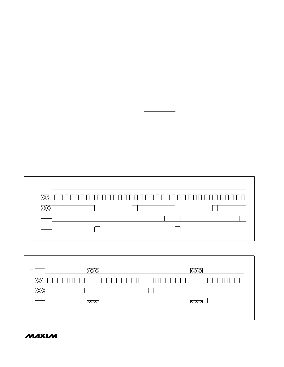
Figure 11a. External Clock Mode, 15 Clocks/Conversion Timing
Figure 11b. External Clock Mode, 16 Clocks/Conversion Timing
Data Framing
The falling edge of CS does not start a conversion.
The first logic high clocked into DIN is interpreted as a
start bit and defines the first bit of the control byte. A
conversion starts on SCLK’s falling edge, after the eighth
bit of the control byte (the PD0 bit) is clocked into DIN.
The start bit is defined as follows:
The first high bit clocked into DIN with CS low any
time the converter is idle; e.g., after VDD is applied.
OR
The first high bit clocked into DIN after bit 5 of a con-
version in progress is clocked onto the DOUT pin.
If CS is toggled before the current conversion is com-
plete, the next high bit clocked into DIN is recognized as
a start bit; the current conversion is terminated, and a
new one is started.
The fastest the MAX146/MAX147 can run with CS held
low between conversions is 15 clocks per conversion.
Figure 11a shows the serial-interface timing necessary to
perform a conversion every 15 SCLK cycles in external
clock mode. If CS is tied low and SCLK is continuous,
guarantee a start bit by first clocking in 16 zeros.
Most microcontrollers (Cs) require that conversions
occur in multiples of 8 SCLK clocks; 16 clocks per con-
version is typically the fastest that a C can drive the
MAX146/MAX147. Figure 11b shows the serial-
interface timing necessary to perform a conversion every
16 SCLK cycles in external clock mode.
Applications Information
Power-On Reset
When power is first applied, and if SHDN is not pulled
low, internal power-on reset circuitry activates the
MAX146/MAX147 in internal clock mode, ready to con-
vert with SSTRB = high. After the power supplies stabi-
lize, the internal reset time is 10s, and no conversions
should be performed during this phase. SSTRB is high
on power-up and, if CS is low, the first logical 1 on DIN
is interpreted as a start bit. Until a conversion takes
place, DOUT shifts out zeros. (Also see Table 4.)
相关PDF资料 |
PDF描述 |
|---|---|
| LLS2G271MELA | CAP ALUM 270UF 400V 20% SNAP |
| 0210490372 | CABLE JUMPER 1.25MM .102M 30POS |
| 380LX332M080K022 | CAP ALUM 3300UF 80V 20% SNAP |
| 0210490371 | CABLE JUMPER 1.25MM .102M 30POS |
| MAX110EVC32-DIP | EVAL KIT FOR MAX110 |
相关代理商/技术参数 |
参数描述 |
|---|---|
| MAX147EVC32-DIP | 功能描述:数据转换 IC 开发工具 MAX147 Eval Kit RoHS:否 制造商:Texas Instruments 产品:Demonstration Kits 类型:ADC 工具用于评估:ADS130E08 接口类型:SPI 工作电源电压:- 6 V to + 6 V |
| MAX147EVKIT-DIP | 功能描述:数据转换 IC 开发工具 MAX147 Eval Kit RoHS:否 制造商:Texas Instruments 产品:Demonstration Kits 类型:ADC 工具用于评估:ADS130E08 接口类型:SPI 工作电源电压:- 6 V to + 6 V |
| MAX14800CCM+ | 功能描述:模拟开关 IC RoHS:否 制造商:Texas Instruments 开关数量:2 开关配置:SPDT 开启电阻(最大值):0.1 Ohms 切换电压(最大): 开启时间(最大值): 关闭时间(最大值): 工作电源电压:2.7 V to 4.5 V 最大工作温度:+ 85 C 安装风格:SMD/SMT 封装 / 箱体:DSBGA-16 |
| MAX14800CCM+T | 功能描述:模拟开关 IC RoHS:否 制造商:Texas Instruments 开关数量:2 开关配置:SPDT 开启电阻(最大值):0.1 Ohms 切换电压(最大): 开启时间(最大值): 关闭时间(最大值): 工作电源电压:2.7 V to 4.5 V 最大工作温度:+ 85 C 安装风格:SMD/SMT 封装 / 箱体:DSBGA-16 |
| MAX14801CCM+ | 功能描述:模拟开关 IC RoHS:否 制造商:Texas Instruments 开关数量:2 开关配置:SPDT 开启电阻(最大值):0.1 Ohms 切换电压(最大): 开启时间(最大值): 关闭时间(最大值): 工作电源电压:2.7 V to 4.5 V 最大工作温度:+ 85 C 安装风格:SMD/SMT 封装 / 箱体:DSBGA-16 |
发布紧急采购,3分钟左右您将得到回复。