- 您现在的位置:买卖IC网 > PDF目录17277 > MAX15026BEVKIT+ (Maxim Integrated Products)KIT EVAL FOR MAX15026 PDF资料下载
参数资料
| 型号: | MAX15026BEVKIT+ |
| 厂商: | Maxim Integrated Products |
| 文件页数: | 15/23页 |
| 文件大小: | 0K |
| 描述: | KIT EVAL FOR MAX15026 |
| 产品培训模块: | Lead (SnPb) Finish for COTS Obsolescence Mitigation Program |
| 标准包装: | 1 |
| 主要目的: | DC/DC,步降 |
| 输出及类型: | 1,非隔离 |
| 输出电压: | 1.5V |
| 电流 - 输出: | 10A |
| 输入电压: | 5 ~ 16 V |
| 稳压器拓扑结构: | 降压 |
| 频率 - 开关: | 600kHz |
| 板类型: | 完全填充 |
| 已供物品: | 板 |
| 已用 IC / 零件: | MAX15026B |
�� �
�
�MAX15026�
�Low-Cost,� Small,� 4.5V� to� 28V� Wide� Operating�
�Range,� DC-DC� Synchronous� Buck� Controller�
�requirements.� Choose� the� small-signal� components� for�
�the� error� amplifier� to� achieve� the� desired� closed-loop�
�bandwidth� and� phase� margin.�
�To� choose� the� appropriate� compensation� network� type,�
�the� power-supply� poles� and� zeros,� the� zero� crossover�
�frequency,� and� the� type� of� the� output� capacitor� must� be�
�determined.�
�In� a� buck� converter,� the� LC� filter� in� the� output� stage� intro-�
�duces� a� pair� of� complex� poles� at� the� following� frequency:�
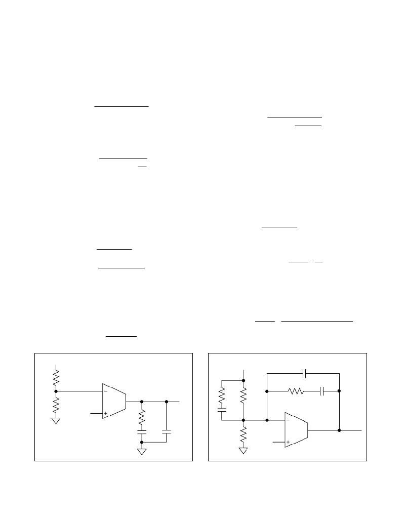
�Type� II� Compensation� Network�
�(Figure� 3)�
�If� f� ZO� is� lower� than� f� O� and� close� to� f� PO� ,� the� phase� lead�
�of� the� capacitor� ESR� zero� almost� cancels� the� phase�
�loss� of� one� of� the� complex� poles� of� the� LC� filter� around�
�the� crossover� frequency.� Use� a� Type� II� compensation�
�network� with� a� midband� zero� and� a� high-frequency�
�pole� to� stabilize� the� loop.� In� Figure� 3,� R� F� and� C� F� intro-�
�duce� a� midband� zero� (f� Z1� ).� R� F� and� C� CF� in� the� Type� II�
�compensation� network� provide� a� high-frequency� pole�
�f� PO� =�
�1�
�2� π� ×� L� OUT� ×� C� OUT�
�(f� P1� ),� which� mitigates� the� effects� of� the� output� high-fre-�
�quency� ripple.�
�Follow� the� instructions� below� to� calculate� the� component�
�The� output� capacitor� introduces� a� zero� at:�
�values� for� the� Type� II� compensation� network� in� Figure� 3:�
�f� ZO� =�
�1�
�2� π� ×� ESR� ×� C� OUT�
�1)� Calculate� the� gain� of� the� modulator� (GAIN� MOD� ),�
�comprised� of� the� regulator’s� pulse-width� modulator,�
�LC� filter,� feedback� divider,� and� associated� circuitry�
�at� the� crossover� frequency:�
�where� ESR� is� the� equivalent� series� resistance� of� the�
��
�output� capacitor.�
�The� loop-gain� crossover� frequency� (f� O� ),� where� the� loop�
�gain� equals� 1� (0dB)� should� be� set� below� 1/10th� of� the�
�GAIN� MOD� =�
�V� IN� ESR�
�V� RAMP� (� 2� π� ×� f� O� ×� L� OUT� )�
��
�V� FB�
�V� OUT�
�f� O� ≤� SW�
�switching� frequency:�
�f�
�10�
�Choosing� a� lower� crossover� frequency� reduces� the�
�effects� of� noise� pick-up� into� the� feedback� loop,� such� as�
�jittery� duty� cycle.�
�To� maintain� a� stable� system,� two� stability� criteria� must�
�be� met:�
�1)� The� phase� shift� at� the� crossover� frequency� f� O� ,� must�
�be� less� than� 180°.� In� other� words,� the� phase� margin�
�of� the� loop� must� be� greater� than� zero.�
�2)� The� gain� at� the� frequency� where� the� phase� shift� is�
�-180°� (gain� margin)� must� be� less� than� 1.�
�where� V� IN� is� the� input� voltage� of� the� regulator,� V� RAMP� is�
�the� amplitude� of� the� ramp� in� the� pulse-width� modulator,�
�V� FB� is� the� FB� input� voltage� set-point� (0.591V� typically,�
�see� the� Electrical� Characteristics� table),� and� V� OUT� is�
�the� desired� output� voltage.�
�The� gain� of� the� error� amplifier� (GAIN� EA� )� in� midband� fre-�
�quencies� is:�
�GAIN� EA� =� g� M� x� R� F�
�where� g� M� is� the� transconductance� of� the� error� amplifier.�
�The� total� loop� gain,� which� is� the� product� of� the� modula-�
�tor� gain� and� the� error� amplifier� gain� at� f� O� ,� is� 1.�
�GAIN� MOD� � GAIN� EA� =� 1�
�So:�
�� � g� M� F� =� 1�
�� R�
�Maintain� a� phase� margin� of� around� 60°� to� achieve� a�
�robust� loop� stability� and� well-behaved� transient�
�response.�
�V� IN�
�V� RAMP�
��
�ESR�
�(� 2� π� ×� f� O� ×� L� OUT� )�
�V� FB�
�V� OUT�
�×� (� 2� π� ×� f� ×� L� )� ×� V�
�R� F� =� RAMP� O� OUT� OUT�
�When� using� an� electrolytic� or� large-ESR� tantalum� output�
�capacitor� the� capacitor� ESR� zero� f� ZO� typically� occurs�
�between� the� LC� poles� and� the� crossover� frequency� f� O�
�(f� PO� <� f� ZO� <� f� O� ).� Choose� Type� II� (PI—proportional-inte-�
�gral)� compensation� network.�
�When� using� a� ceramic� or� low-ESR� tantalum� output�
�capacitor,� the� capacitor� ESR� zero� typically� occurs�
�Solving� for� R� F� :�
�V�
�V� FB� � V� IN� � g� M� � ESR�
�2)� Set� a� midband� zero� (f� Z1� )� at� 0.75� x� f� PO� (to� cancel�
�one� of� the� LC� poles):�
�above� the� desired� crossover� frequency� f� O� ,� that� is� f� PO� <�
�f� O� <� f� ZO� .� Choose� Type� III� (PID—proportional,� integral,�
�and� derivative)� compensation� network.�
�Maxim� Integrated�
�f� Z� 1� =�
�1�
�2� π� ×� R� F� ×� C� F�
�=� 0� .� 75� � f� PO�
�15�
�相关PDF资料 |
PDF描述 |
|---|---|
| GEM30DTBN | CONN EDGECARD 60POS R/A .156 SLD |
| 592D337X96R3V2T035 | CAP TANT 330UF 6.3V 10% SMD |
| R1D10-1512 | CONV DC/DC 1W 15VIN +/-12VOUT |
| MCZ33291LEG | IC SWITCH 8X LOSIDE W/SPI 24SOIC |
| FAN3122CMX | IC GATE DVR SGL 9A HS 8-SOIC |
相关代理商/技术参数 |
参数描述 |
|---|---|
| MAX15026BEVKIT+ | 功能描述:电源管理IC开发工具 MAX15026B Eval Kit RoHS:否 制造商:Maxim Integrated 产品:Evaluation Kits 类型:Battery Management 工具用于评估:MAX17710GB 输入电压: 输出电压:1.8 V |
| MAX15026CATD+ | 功能描述:DC/DC 开关控制器 4.5-28V Synchronous Buck Controller RoHS:否 制造商:Texas Instruments 输入电压:6 V to 100 V 开关频率: 输出电压:1.215 V to 80 V 输出电流:3.5 A 输出端数量:1 最大工作温度:+ 125 C 安装风格: 封装 / 箱体:CPAK |
| MAX15026CATD+T | 功能描述:DC/DC 开关控制器 4.5-28V Synchronous Buck Controller RoHS:否 制造商:Texas Instruments 输入电压:6 V to 100 V 开关频率: 输出电压:1.215 V to 80 V 输出电流:3.5 A 输出端数量:1 最大工作温度:+ 125 C 安装风格: 封装 / 箱体:CPAK |
| MAX15026CETD+ | 功能描述:DC/DC 开关控制器 4.5-28V Synchronous Buck Controller RoHS:否 制造商:Texas Instruments 输入电压:6 V to 100 V 开关频率: 输出电压:1.215 V to 80 V 输出电流:3.5 A 输出端数量:1 最大工作温度:+ 125 C 安装风格: 封装 / 箱体:CPAK |
| MAX15026CETD+G1D | 制造商:Maxim Integrated Products 功能描述:LOW-COST, SMALL, 4.5V TO 28V WIDE OPERATING RANGE, DC-DC SYN - Rail/Tube |
发布紧急采购,3分钟左右您将得到回复。