- 您现在的位置:买卖IC网 > PDF目录1836 > MAX15049ETJ+ (Maxim Integrated Products)IC CTRLR PWM STP-DN TRIPL 32WQFN PDF资料下载
参数资料
| 型号: | MAX15049ETJ+ |
| 厂商: | Maxim Integrated Products |
| 文件页数: | 11/31页 |
| 文件大小: | 0K |
| 描述: | IC CTRLR PWM STP-DN TRIPL 32WQFN |
| 产品培训模块: | Lead (SnPb) Finish for COTS Obsolescence Mitigation Program |
| 标准包装: | 1 |
| 应用: | 电源控制器,序列发生器 |
| 电源电压: | 4.7 V ~ 23 V |
| 电流 - 电源: | 6mA |
| 工作温度: | -40°C ~ 85°C |
| 安装类型: | 表面贴装 |
| 封装/外壳: | 32-WFQFN 裸露焊盘 |
| 供应商设备封装: | 32-TQFN-EP(5x5) |
| 包装: | 管件 |
第1页第2页第3页第4页第5页第6页第7页第8页第9页第10页当前第11页第12页第13页第14页第15页第16页第17页第18页第19页第20页第21页第22页第23页第24页第25页第26页第27页第28页第29页第30页第31页
�� �
�
�MAX15048/MAX15049�
�Triple-Output� Buck� Controllers�
�with� Tracking/Sequencing�
�Pin� Description� (continued)�
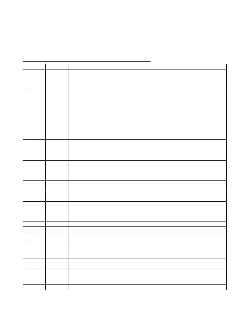
�PIN�
�12�
�13�
�14�
�15�
�16�
�17�
�18�
�19�
�20�
�21�
�22�
�23�
�24�
�25�
�26�
�27�
�28�
�29�
�30�
�31�
�32�
�—�
�Maxim� Integrated�
�NAME�
�PGOOD�
�COMP1�
�FB1�
�EN1�
�BST1�
�DH1�
�LX1�
�DREG1�
�DL1�
�PGND1�
�COMP3�
�FB3�
�EN3�
�BST3�
�DH3�
�LX3�
�DREG3�
�DL3�
�PGND3�
�IN�
�REG�
�EP�
�FUNCTION�
�Controller� Power-Good� Output.� Pull� up� PGOOD� with� a� resistor� to� a� positive� voltage� below� 5.5V.�
�For� the� MAX15048,� PGOOD� output� releases� when� all� three� V� FB_� voltages� are� above� 0.55V.� For� the�
�MAX15049,� PGOOD� output� releases� when� all� three� controllers� are� out� of� prebias� and� all� three� V� FB_�
�voltages� are� above� 0.55V.�
�Controller� 1� Transconductance� Error-Amplifier� Output.� Connect� COMP1� to� the� compensation�
�feedback� network� of� output� 1.�
�Controller� 1� Feedback� Regulation� Point.� Connect� to� the� center� tap� of� a� resistive� voltage-divider� from�
�the� converter� output� to� SGND� to� set� the� output� voltage.� The� FB1� voltage� regulates� to� 0.6V� (typ).�
�Controller� 1� Enable� Input.� For� tracking� (MAX15048),� EN1� must� be� above� 0.6V,� V� EN-TH� ,� for� the� PWM�
�controller� to� start� outputs� 1,� 2,� and� 3.� Controller� 1� is� the� master.� Use� the� master� as� the� highest� output�
�voltage� in� a� coincident� tracking� configuration.� For� the� MAX15049,� EN1� must� be� above� 0.6V� for� the�
�PWM� controller� to� start� output� 1.�
�Controller� 1� High-Side� Gate-Driver� Supply.� Connect� a� 0.1� F� F� ceramic� capacitor� from� BST1� to� LX1.�
�Controller� 1� High-Side� Gate-Driver� Output.� DH1� drives� the� gate� of� the� high-side� MOSFET.�
�Controller� 1� High-Side� MOSFET� Source� Connection/Synchronous� MOSFET� Drain� Connection.�
�Connect� the� inductor� and� the� negative� side� of� the� boost� capacitor� to� LX1.�
�Controller� 1� Low-Side� Gate-Driver� Supply.� Connect� externally� to� REG� through� a� 1� I� to� 4.7� I� resistor.�
�Connect� a� minimum� of� 0.22� F� F� ceramic� capacitor� from� DREG1� to� PGND1.�
�Controller 1 Low-Side Gate-Driver Output. DL1 is the gate-driver output for the synchronous MOSFET.�
�Controller� 1� Power� Ground.� Connect� the� input� filter� capacitor’s� negative� terminal,� the� source� of� the�
�synchronous� MOSFET,� and� the� output� filter� capacitor’s� return� to� PGND1.� Connect� to� SGND� at� a�
�single� point� near� the� input� capacitor� return� terminal.�
�Controller� 3� Transconductance� Error-Amplifier� Output.� Connect� COMP3� to� the� compensation�
�feedback� network� of� output� 3.�
�Controller� 3� Feedback� Regulation� Point.� Connect� to� the� center� tap� of� a� resistive� voltage-divider� from�
�the� converter� output� to� SGND� to� set� the� output� voltage.� The� FB3� voltage� regulates� to� 0.6V� (typ).�
�Controller� 3� Enable/Tracking� Input.� See� Figure� 2.� When� tracking� (MAX15048),� connect� the� same�
�resistive� voltage-divider� used� for� FB3� from� output� 1� to� EN3� to� SGND� for� coincident� tracking.� Connect�
�EN3� to� analog� ground� for� ratiometric� tracking.� When� sequencing� (MAX15049),� EN3� must� be� above�
�0.6V� for� PWM� controller� 3� to� start.�
�Controller� 3� High-Side� Gate-Driver� Supply.� Connect� a� 0.1� F� F� ceramic� capacitor� from� BST3� to� LX3.�
�Controller� 3� High-Side� Gate-Driver� Output.� DH3� drives� the� gate� of� the� high-side� MOSFET.�
�Controller� 3� High-Side� MOSFET� Source� Connection/Synchronous� MOSFET� Drain� Connection.�
�Connect� the� inductor� and� the� negative� side� of� the� boost� capacitor� to� LX3.�
�Controller� 3� Low-Side� Gate-Driver� Supply.� Connect� externally� to� REG� through� a� 1� I� to� 4.7� I� resistor.�
�Connect� a� minimum� of� 0.22� F� F� ceramic� capacitor� from� DREG3� to� PGND3.�
�Controller 3 Low-Side Gate-Driver Output. DL3 is the gate-driver output for the synchronous MOSFET.�
�Controller� 3� Power� Ground.� Connect� the� input� filter� capacitor’s� negative� terminal,� the� source� of� the�
�synchronous� MOSFET,� and� the� output� filter� capacitor’s� return� to� PGND3.�
�Supply� Input� Connection.� Connect� to� an� external� voltage� source� from� 4.7V� to� 23V.� For� 4.5V� to� 5.5V�
�input� applications,� connect� IN� and� REG� together.�
�5V� Regulator� Output.� Bypass� with� a� 2.2� F� F� ceramic� capacitor� to� SGND.�
�Exposed� Pad.� Solder� the� exposed� pad� to� a� large� SGND� plane� to� improve� thermal� dissipation.�
�11�
�相关PDF资料 |
PDF描述 |
|---|---|
| MAX15053AEWL+T | IC REG BUCK SYNC ADJ 2A 9WLP |
| MAX15058EWL+T | IC REG BUCK SYNC ADJ 3A 9WLP |
| MAX15059BETE+ | IC REG CONV 76V APD 16TQFN |
| MAX15061ATE+ | IC BOOST CONV/CURR MON 16-TQFN |
| MAX15066EWE+T | IC REG BUCK SYNC ADJ 4A 16WLP |
相关代理商/技术参数 |
参数描述 |
|---|---|
| MAX15049ETJ+ | 功能描述:DC/DC 开关控制器 1.2MHz Triple Buck w/Tracking RoHS:否 制造商:Texas Instruments 输入电压:6 V to 100 V 开关频率: 输出电压:1.215 V to 80 V 输出电流:3.5 A 输出端数量:1 最大工作温度:+ 125 C 安装风格: 封装 / 箱体:CPAK |
| MAX15049ETJ+ | 制造商:Maxim Integrated Products 功能描述:IC BUCK CNTRL TRIPLE 32WQFN 制造商:Maxim Integrated Products 功能描述:IC, BUCK, CNTRL, TRIPLE, 32WQFN |
| MAX15049ETJ+ | 制造商:Maxim Integrated Products 功能描述:IC PWM STEP-DOWN DC/DC CONVER |
| MAX15049ETJ+T | 功能描述:DC/DC 开关控制器 1.2MHz Triple Buck w/Tracking RoHS:否 制造商:Texas Instruments 输入电压:6 V to 100 V 开关频率: 输出电压:1.215 V to 80 V 输出电流:3.5 A 输出端数量:1 最大工作温度:+ 125 C 安装风格: 封装 / 箱体:CPAK |
| MAX15049EVKIT+ | 功能描述:电源管理IC开发工具 MAX15049 Eval Kit RoHS:否 制造商:Maxim Integrated 产品:Evaluation Kits 类型:Battery Management 工具用于评估:MAX17710GB 输入电压: 输出电压:1.8 V |
发布紧急采购,3分钟左右您将得到回复。