- 您现在的位置:买卖IC网 > PDF目录1836 > MAX15049ETJ+ (Maxim Integrated Products)IC CTRLR PWM STP-DN TRIPL 32WQFN PDF资料下载
参数资料
| 型号: | MAX15049ETJ+ |
| 厂商: | Maxim Integrated Products |
| 文件页数: | 19/31页 |
| 文件大小: | 0K |
| 描述: | IC CTRLR PWM STP-DN TRIPL 32WQFN |
| 产品培训模块: | Lead (SnPb) Finish for COTS Obsolescence Mitigation Program |
| 标准包装: | 1 |
| 应用: | 电源控制器,序列发生器 |
| 电源电压: | 4.7 V ~ 23 V |
| 电流 - 电源: | 6mA |
| 工作温度: | -40°C ~ 85°C |
| 安装类型: | 表面贴装 |
| 封装/外壳: | 32-WFQFN 裸露焊盘 |
| 供应商设备封装: | 32-TQFN-EP(5x5) |
| 包装: | 管件 |
第1页第2页第3页第4页第5页第6页第7页第8页第9页第10页第11页第12页第13页第14页第15页第16页第17页第18页当前第19页第20页第21页第22页第23页第24页第25页第26页第27页第28页第29页第30页第31页
�� �
�
�MAX15048/MAX15049�
�Triple-Output� Buck� Controllers�
�with� Tracking/Sequencing�
�Consequently,� peak� currents� and� I� 2� R� losses� are� lower�
�at� higher� switching� frequencies,� but� core� losses,� gate-�
�IN�
�CURRENT� LIMIT�
�COUNT� OF� 8�
�N� CL�
�CLR�
�INITIATE� HICCUP�
�TIMEOUT�
�N� HT�
�charge� currents,� and� switching� losses� increase.�
�Effective� Input� Voltage� Range�
�Although� the� MAX15048/MAX15049� converters� can�
�operate� from� input� supplies� ranging� from� 4.7V� to� 23V,�
�the� input� voltage� range� can� be� effectively� limited� by� the�
�duty-cycle� limitations� for� a� given� output� voltage.� The�
�IN�
�COUNT� OF� 3�
�N� CLR�
�CLR�
�maximum� input� voltage� is� limited� by� the� minimum� on-�
�time� (t� ON(MIN)� ):�
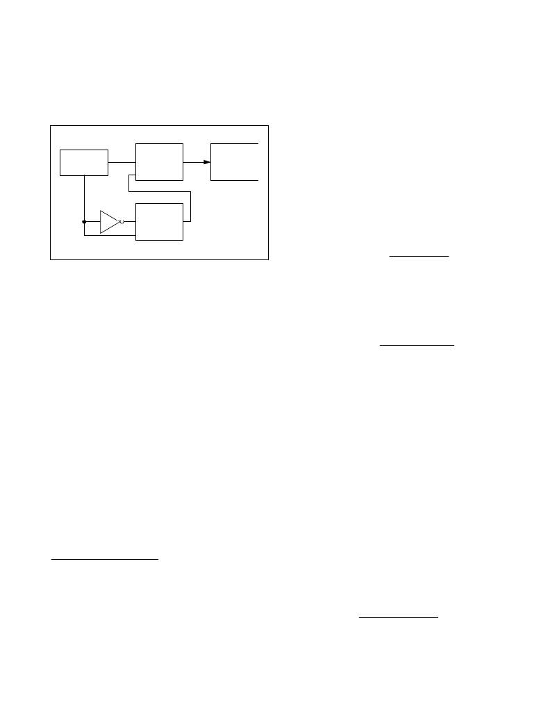
�Figure� 3.� Hiccup-Mode� Block� Diagram�
�V� IN(MAX)� ≤�
�V� OUT_�
�t� ON(MIN)� � f� SW�
�just� before� the� beginning� of� a� new� PWM� cycle,� the� con-�
�troller� skips� that� cycle.� During� severe� overload� or� short-�
�circuit� conditions,� the� switching� frequency� of� the� device�
�appears� to� decrease� because� the� on-time� of� the� low-side�
�MOSFET� extends� beyond� a� clock� cycle.�
�where� t� ON(MIN)� is� 75ns.�
�The� minimum� input� voltage� is� limited� by� the� maximum�
�duty� cycle� and� is� calculated� using� the� following� equa-�
�tion:�
�If� the� current-limit� threshold� is� exceeded� for� more� than�
�eight� cumulative� clock� cycles� (N� CL� ),� the� device� shuts�
�down� (both� DH_� and� DL_� are� pulled� low)� for� 4096� clock�
�V� IN(MIN)� =�
�V� OUT_�
�1-(t� OFF(MIN)� � f� SW� )�
�L� =� OUT_� IN� OUT_�
�cycles� (hiccup� timeout)� and� then� restarts� with� a� soft-�
�start� sequence.� If� three� consecutive� cycles� pass� without�
�a� current-limit� event,� the� count� of� N� CL� is� cleared� (see�
�Figure� 3).� Hiccup� mode� protects� the� circuit� against� a�
�continuous� output� short� circuit.�
�Thermal-Overload� Protection�
�The� MAX15048/MAX15049� feature� an� integrated� ther-�
�mal-overload� protection� with� temperature� hysteresis.�
�Thermal-overload� protection� limits� the� total� power� dis-�
�sipation� in� the� device� and� protects� it� in� the� event� of� an�
�extended� thermal-fault� condition.� When� the� die� tempera-�
�ture� exceeds� +160� N� C� (typ),� an� internal� thermal� sensor�
�shuts� down� the� device,� turning� off� the� power� MOSFETs�
�and� allowing� the� die� to� cool.� After� the� die� temperature�
�falls� by� +20� N� C� (typ),� the� part� restarts� with� a� soft-start�
�sequence.�
�Design� Procedure�
�Setting� the� Switching� Frequency�
�Connect� a� 15.625k� I� to� 93.75k� I� resistor� from� RT� to�
�SGND� to� program� the� switching� frequency� from� 200kHz�
�to� 1.2MHz.� Calculate� the� switching� frequency� using� the�
�following� equation:�
�f� SW� (kHz)� =� 12.8� O� R� RT� (k� I� )�
�Higher� switching� frequencies� allow� designs� with�
�lower� inductor� values� and� less� output� capacitance.�
�Maxim� Integrated�
�where� t� OFF(MIN)� typically� is� equal� to� 300ns.�
�Inductor� Selection�
�Three� key� inductor� parameters� must� be� specified� for�
�operation� with� the� MAX15048/MAX15049:� inductance�
�value� (L),� inductor� saturation� current� (I� SAT� ),� and� induc-�
�tor� series� resistance� (DCR).� The� minimum� required�
�inductance� is� a� function� of� operating� frequency,� input-to-�
�output� voltage� differential,� and� the� peak-to-peak� inductor�
�current� (� D� I� P-P� ).� Higher� D� I� P-P� allows� for� a� lower� inductor�
�value.� A� lower� inductance� value� minimizes� size� and�
�cost� and� improves� large-signal� and� transient� response.�
�However,� efficiency� is� reduced� due� to� higher� peak� cur-�
�rents� and� higher� peak-to-peak� output-voltage� ripple� for�
�the� same� output� capacitor.� A� higher� inductance� increas-�
�es� efficiency� by� reducing� the� ripple� current;� however,�
�resistive� losses� due� to� extra� wire� turns� can� exceed� the�
�benefit� gained� from� lower� ripple� current� levels,� especial-�
�ly� when� the� inductance� is� increased� without� also� allow-�
�ing� for� larger� inductor� dimensions.� A� good� rule� of� thumb�
�is� to� choose� D� I� P-P� equal� to� 30%� of� the� full� load� current.�
�Calculate� the� inductance� using� the� following� equation:�
�V (V - V )�
�V� IN� � f� SW� � ?� I� P-P�
�V� IN� and� V� OUT_� are� typical� values� so� that� efficiency� is�
�optimum� for� typical� conditions.� The� switching� frequency�
�19�
�相关PDF资料 |
PDF描述 |
|---|---|
| MAX15053AEWL+T | IC REG BUCK SYNC ADJ 2A 9WLP |
| MAX15058EWL+T | IC REG BUCK SYNC ADJ 3A 9WLP |
| MAX15059BETE+ | IC REG CONV 76V APD 16TQFN |
| MAX15061ATE+ | IC BOOST CONV/CURR MON 16-TQFN |
| MAX15066EWE+T | IC REG BUCK SYNC ADJ 4A 16WLP |
相关代理商/技术参数 |
参数描述 |
|---|---|
| MAX15049ETJ+ | 功能描述:DC/DC 开关控制器 1.2MHz Triple Buck w/Tracking RoHS:否 制造商:Texas Instruments 输入电压:6 V to 100 V 开关频率: 输出电压:1.215 V to 80 V 输出电流:3.5 A 输出端数量:1 最大工作温度:+ 125 C 安装风格: 封装 / 箱体:CPAK |
| MAX15049ETJ+ | 制造商:Maxim Integrated Products 功能描述:IC BUCK CNTRL TRIPLE 32WQFN 制造商:Maxim Integrated Products 功能描述:IC, BUCK, CNTRL, TRIPLE, 32WQFN |
| MAX15049ETJ+ | 制造商:Maxim Integrated Products 功能描述:IC PWM STEP-DOWN DC/DC CONVER |
| MAX15049ETJ+T | 功能描述:DC/DC 开关控制器 1.2MHz Triple Buck w/Tracking RoHS:否 制造商:Texas Instruments 输入电压:6 V to 100 V 开关频率: 输出电压:1.215 V to 80 V 输出电流:3.5 A 输出端数量:1 最大工作温度:+ 125 C 安装风格: 封装 / 箱体:CPAK |
| MAX15049EVKIT+ | 功能描述:电源管理IC开发工具 MAX15049 Eval Kit RoHS:否 制造商:Maxim Integrated 产品:Evaluation Kits 类型:Battery Management 工具用于评估:MAX17710GB 输入电压: 输出电压:1.8 V |
发布紧急采购,3分钟左右您将得到回复。