- 您现在的位置:买卖IC网 > PDF目录20779 > MAX16831ATJ+ (Maxim Integrated)IC LED DRIVR HIGH BRIGHT 32-TQFN PDF资料下载
参数资料
| 型号: | MAX16831ATJ+ |
| 厂商: | Maxim Integrated |
| 文件页数: | 12/19页 |
| 文件大小: | 0K |
| 描述: | IC LED DRIVR HIGH BRIGHT 32-TQFN |
| 产品培训模块: | Lead (SnPb) Finish for COTS Obsolescence Mitigation Program |
| 标准包装: | 60 |
| 拓扑: | PWM,降压(降压),升压(升压) |
| 输出数: | 1 |
| 内部驱动器: | 无 |
| 类型 - 主要: | 车载 |
| 类型 - 次要: | 高亮度 LED(HBLED),RGB |
| 频率: | 125kHz ~ 600kHz |
| 电源电压: | 5.5 V ~ 76 V |
| 安装类型: | 表面贴装 |
| 封装/外壳: | 32-WFQFN 裸露焊盘 |
| 供应商设备封装: | 32-TQFN-EP(5x5) |
| 包装: | 管件 |
| 工作温度: | -40°C ~ 125°C |
| 产品目录页面: | 1425 (CN2011-ZH PDF) |
�� �
�
�MAX16831�
�High-Voltage,� High-Power� LED� Driver� with�
�Analog� and� PWM� Dimming� Control�
�Connect� the� clock� signal� to� the� RTSYNC� input.� The�
�MAX16831� synchronizes� to� the� external� clock� signal�
�after� the� detection� of� five� successive� clock� edges� at�
�RTSYNC.�
�A� buffered� clock� output,� CLKOUT,� is� capable� of� driving�
�the� RTSYNC� input� of� an� external� PWM� controller� for�
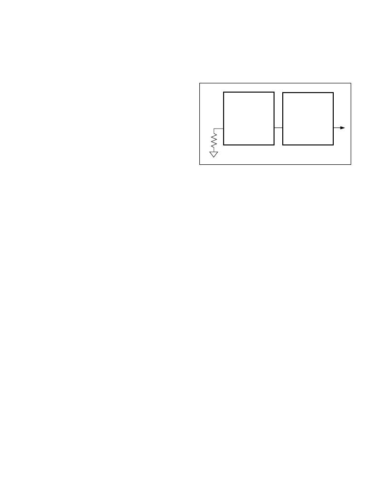
�MASTER/PEER�
�MAX16831�
�SLAVE/PEER�
�MAX16831�
�multichannel� applications.� CLKOUT� is� capable� of� dri-�
�RTSYNC�
�CLKOUT�
�RTSYNC�
�CLKOUT�
�ving� capacitive� loads� up� to� 500pF.�
�Multichannel� Configuration�
�The� MAX16831� is� capable� of� multichannel� operation.�
�Connect� CLKOUT� to� the� SYNC� input� of� an� external�
�device� to� use� the� MAX16831� as� a� master� clock� signal.�
�Connect� an� external� clock� signal� to� RTSYNC� to� config-�
�ure� the� MAX16831� as� a� slave.� To� setup� two� or� more�
�MAX16831� devices� in� a� daisy-chain/peer-to-peer� con-�
�figuration,� drive� the� RTSYNC� input� of� one� MAX16831�
�with� the� CLKOUT� buffer� of� another� (Figure� 3).�
�ILIM� and� HICCUP� Comparator�
�R� SENSE� sets� the� peak� current� through� the� inductor� for�
�switching.� The� differential� voltage� across� R� SENSE� is�
�compared� to� the� 200mV� voltage� trip� limit� of� the� current-�
�limit� comparator,� ILIM.� Set� the� current� limit� 20%� higher�
�than� the� peak� switch� current� at� the� rated� output� power�
�and� minimum� voltage.� Use� the� following� equation� to�
�calculate� R� SENSE� :�
�R� SENSE� =� V� SENSE� /� (1.2� x� I� PEAK� )�
�where� V� SENSE� is� the� 200mV� differential� voltage�
�between� SNS+� and� SNS-� and� I� PEAK� is� the� peak� induc-�
�tor� current� at� full� load� and� minimum� input� voltage.�
�When� the� voltage� drop� across� R� SENSE� exceeds� the�
�ILIM� threshold,� the� MOSFET� driver� (DRV)� terminates�
�the� on-cycle� and� turns� the� switch� off,� reducing� the� cur-�
�rent� through� the� inductor.� The� FET� is� turned� back� on� at�
�the� beginning� of� the� next� switching� cycle.�
�When� the� voltage� across� R� SENSE� exceeds� the� 300mV�
�(typ)� HICCUP� threshold,� the� HIC� comparator� terminates�
�the� on-cycle� of� the� device,� turning� the� switching�
�MOSFET� off.� Following� a� startup� delay� of� 4ms� (typ),� the�
�MAX16831� re-initiates� soft-start.� The� device� will� contin-�
�ue� to� operate� in� HICCUP� mode� until� the� overcurrent�
�condition� is� removed.�
�A� built-in� 40ns� leading-edge� blanking� circuit� of� the� cur-�
�rent-sense� signal� prevents� these� comparators� from� pre-�
�maturely� terminating� the� on-cycle� of� the� external�
�switching� MOSFET� (Q� S� ).� In� some� cases,� this� blanking�
�time� may� not� be� adequate� and� an� additional� RC� filter�
�may� be� required� to� prevent� spurious� turn-off.�
�12�
�R� T�
�Figure� 3.� Master-Slave/Peer-Peer� Clock� Configuration�
�Load� Current� Sense�
�The� load-sense� resistor,� R� CS� ,� monitors� the� current�
�through� the� LEDs.� The� internal� floating� current-sense�
�amplifier,� CSA,� measures� the� differential� voltage� across�
�R� CS� ,� and� generates� a� voltage� proportional� to� the� LED�
�current� through� R� CS� at� CS.� This� voltage� on� CS� is�
�referred� to� AGND.� The� closed� loop� regulates� the� LED�
�current� to� a� value,� I� LED� ,� given� by� the� following� equation:�
�I� LED� =� 0.107V� /� R� CS�
�Slope� Compensation�
�The� MAX16831� uses� an� internal� ramp� generator� for�
�slope� compensation.� The� internal� ramp� signal� is� reset�
�to� zero� at� the� beginning� of� each� cycle� and� has� a� peak-�
�to-peak� voltage� of� 120mV� per� switching� cycle.� Use� an�
�external� resistor,� R� T� ,� to� set� the� switching� frequency,�
�f� SW� ,� and� calculate� the� slope� of� the� compensating� ramp,�
�m� SLOPE� ,� using� the� following� equation:�
�m� SLOPE� =� 120� x� f� SW� [mV/s]�
�where� f� SW� is� the� switching� frequency� in� Hz.� When� the�
�MAX16831� is� synchronized� to� an� external� clock,� the�
�slope� compensation� ramp� has� a� slope� of� 15mV/μs.�
�Internal� Voltage-Error� Amplifier� (EAMP)�
�The� MAX16831� includes� a� built-in� voltage� amplifier,�
�with� tri-state� output,� which� can� be� used� to� close� the�
�feedback� loop.� The� buffered� output� current-sense� sig-�
�nal� appears� at� CS,� which� is� connected� to� the� inverting�
�input,� FB,� of� the� error� amplifier� through� resistor� R� 1� .� The�
�noninverting� input� is� connected� to� an� internally� trimmed�
�current� reference.�
�The� output� of� the� error� amplifier� is� controlled� by� the� sig-�
�nal� applied� to� DIM.� When� DIM� is� high,� the� output� of� the�
�amplifier� is� connected� to� COMP.� The� amplifier� output� is�
�open� when� DIM� is� low.� This� enables� the� integrating�
�Maxim� Integrated�
�相关PDF资料 |
PDF描述 |
|---|---|
| GEC05DREI-S93 | CONN EDGECARD 10POS .100 EYELET |
| TAJE108M004RNJ | CAP TANT 1000UF 4V 20% 2917 |
| MSL3162BT-R | IC LED DRVR 16 CHAN PWM 40TQFN |
| EEC08DRYS-S93 | CONN EDGECARD 16POS DIP .100 SLD |
| TAJE108M002RNJ | CAP TANT 1000UF 2.5V 20% 2917 |
相关代理商/技术参数 |
参数描述 |
|---|---|
| MAX16831ATJ/V+ | 功能描述:LED照明驱动器 w/Analog & PWM Dimming Control RoHS:否 制造商:STMicroelectronics 输入电压:11.5 V to 23 V 工作频率: 最大电源电流:1.7 mA 输出电流: 最大工作温度: 安装风格:SMD/SMT 封装 / 箱体:SO-16N |
| MAX16831ATJ/V+T | 功能描述:LED照明驱动器 w/Analog & PWM Dimming Control RoHS:否 制造商:STMicroelectronics 输入电压:11.5 V to 23 V 工作频率: 最大电源电流:1.7 mA 输出电流: 最大工作温度: 安装风格:SMD/SMT 封装 / 箱体:SO-16N |
| MAX16831ATJ+ | 功能描述:LED照明驱动器 w/Analog & PWM Dimming Control RoHS:否 制造商:STMicroelectronics 输入电压:11.5 V to 23 V 工作频率: 最大电源电流:1.7 mA 输出电流: 最大工作温度: 安装风格:SMD/SMT 封装 / 箱体:SO-16N |
| MAX16831ATJ+T | 功能描述:LED照明驱动器 w/Analog & PWM Dimming Control RoHS:否 制造商:STMicroelectronics 输入电压:11.5 V to 23 V 工作频率: 最大电源电流:1.7 mA 输出电流: 最大工作温度: 安装风格:SMD/SMT 封装 / 箱体:SO-16N |
| MAX16831EVKIT+ | 功能描述:LED 照明开发工具 MAX16831 Eval Kit RoHS:否 制造商:Fairchild Semiconductor 产品:Evaluation Kits 用于:FL7732 核心: 电源电压:120V 系列: 封装: |
发布紧急采购,3分钟左右您将得到回复。