- 您现在的位置:买卖IC网 > PDF目录1838 > MAX1685EEE-T (Maxim Integrated Products)IC REG BUCK SYNC 3.3V/ADJ 16QSOP PDF资料下载
参数资料
| 型号: | MAX1685EEE-T |
| 厂商: | Maxim Integrated Products |
| 文件页数: | 13/14页 |
| 文件大小: | 0K |
| 描述: | IC REG BUCK SYNC 3.3V/ADJ 16QSOP |
| 产品培训模块: | Lead (SnPb) Finish for COTS Obsolescence Mitigation Program |
| 标准包装: | 2,500 |
| 类型: | 降压(降压) |
| 输出类型: | 两者兼有 |
| 输出数: | 1 |
| 输出电压: | 3.3V,1.25 V ~ 14 V |
| 输入电压: | 2.7 V ~ 14 V |
| PWM 型: | 电流模式 |
| 频率 - 开关: | 600kHz |
| 电流 - 输出: | 1A |
| 同步整流器: | 是 |
| 工作温度: | -40°C ~ 85°C |
| 安装类型: | 表面贴装 |
| 封装/外壳: | 16-SSOP(0.154",3.90mm 宽) |
| 包装: | 带卷 (TR) |
| 供应商设备封装: | 16-QSOP |
�� �
�
�Low-Noise,� 14V� Input,� 1A,� PWM�
�Step-Down� Converters�
�Inverting� Output�
�Interchanging� the� ground� and� V� OUT� connections� yields�
�a� negative� voltage� supply� (Figure� 4).� The� component�
�selections� are� the� same� as� for� a� positive� voltage� con-�
�verter.� The� absolute� maximum� ratings� limit� the� output�
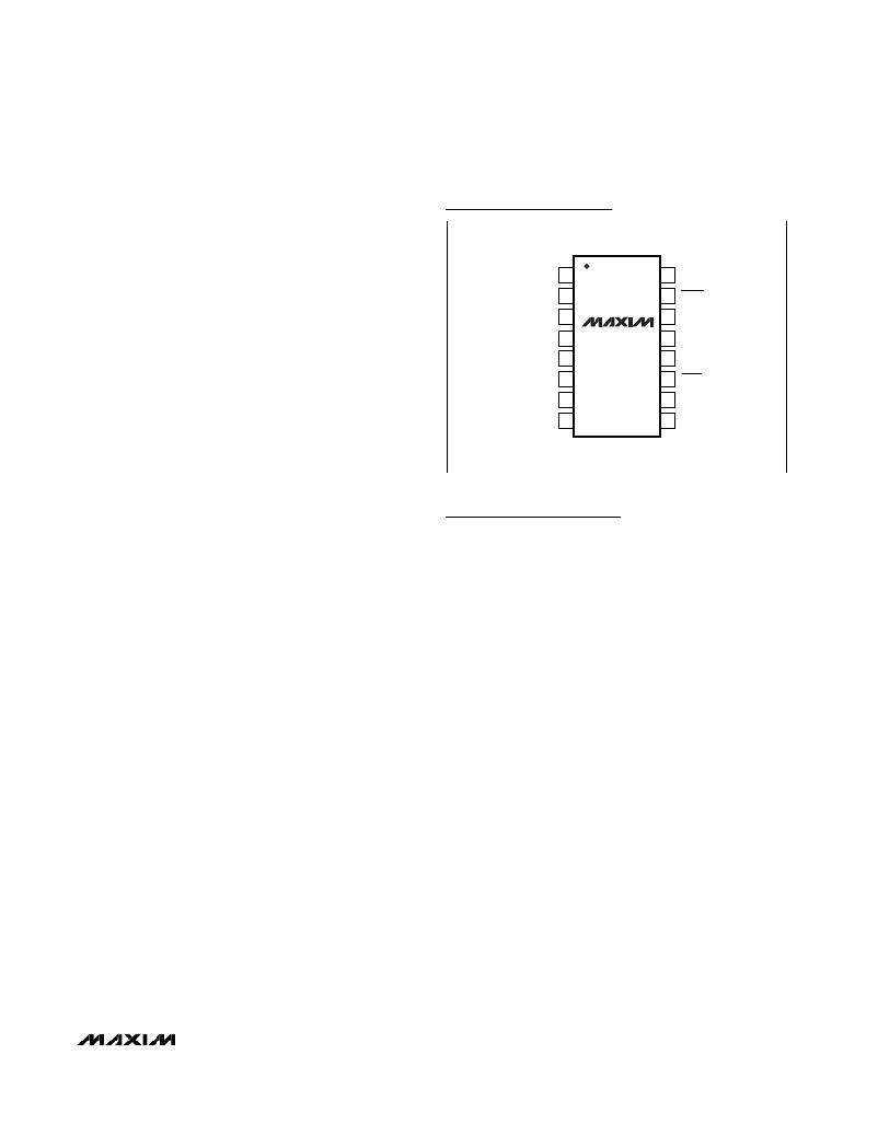
�TOP� VIEW�
�Pin� Configuration�
�voltage� range� to� -1.25V� to� -5.5V� and� the� maximum�
�input� voltage� range� to� 14V� -� ?� V� OUT� ?� .�
�PC� Board� Layout�
�CVH� 1�
�AIN� 2�
�IN� 3�
�16� PGND�
�15� SHDN�
�14� LX�
�High� switching� frequencies� and� large� peak� currents�
�make� PC� board� layout� a� very� important� part� of� design.�
�Poor� design� can� result� in� excessive� EMI� on� the� feed-�
�back� paths� and� voltage� gradients� in� the� ground� plane,�
�both� of� which� result� in� instability� or� regulation� errors.�
�Power� components� such� as� the� MAX1684/MAX1685�
�CVL� 4�
�AGND� 5�
�REF� 6�
�FB� 7�
�MAX1684�
�MAX1685�
�13� LX�
�12� BOOT�
�11� STBY�
�10� ILIM/SS�
�inductor,� input� filter� capacitor,� and� output� filter� capacitor�
�CC� 8�
�9�
�SYNC/PWM�
�should� be� placed� as� close� together� as� possible,� and�
�their� traces� kept� short,� direct,� and� wide,� Connect� their�
�ground� nodes� in� a� star-ground� configuration.� Keep� the�
�extra� copper� on� the� board� and� integrate� into� ground� as�
�a� pseudo-ground� plane.�
�When� using� external� feedback,� the� feedback� network�
�should� be� close� to� FB,� within� 0.2� inch� (5mm),� and� the�
�output� voltage� feedback� should� be� tapped� as� close� to�
�the� output� capacitor� as� possible.� Keep� noisy� traces,�
�such� as� those� from� LX,� away� from� the� voltage� feedback�
�network.� Separate� the� noisy� traces� by� grounded� cop-�
�per.� Place� the� small� bypass� capacitors� within� 0.2� inch�
�(5mm)� of� their� respective� inputs.� The� MAX1684� evalua-�
�tion� kit� manual� illustrates� an� example� PC� board� layout,�
�routing,� and� pseudo-ground� plane.�
�Connect� AIN� to� IN� with� a� short� (0.2� inch)� metal� trace� or� a�
�1� ?� resistor� and� bypass� AIN� to� PGND� with� a� 0.1μF� capac-�
�itor.� This� acts� as� a� lowpass� filter� to� reduce� noise� at� AIN.�
�QSOP�
�Chip� Information�
�TRANSISTOR� COUNT:� 2061�
�______________________________________________________________________________________�
�13�
�相关PDF资料 |
PDF描述 |
|---|---|
| MAX1686HEUA | IC CHRG PUMP FOR SIM CARD 8-UMAX |
| MAX1688ESA+T | IC REG BOOST SYNC ADJ 2.5A 8SOIC |
| MAX16903SAUE50/V+ | IC REG BUCK SYNC 5V 1A 16TSSOP |
| MAX16904RAUE18/V+ | IC REG BUCK SYNC 1.8V 16TSSOP |
| MAX16907RAUE/V+ | IC REG BUCK SYNC ADJ 3A 16TSSOP |
相关代理商/技术参数 |
参数描述 |
|---|---|
| MAX1685EVKIT | 功能描述:电源管理IC开发工具 Evaluation Kit for the MAX1684 MAX1685 RoHS:否 制造商:Maxim Integrated 产品:Evaluation Kits 类型:Battery Management 工具用于评估:MAX17710GB 输入电压: 输出电压:1.8 V |
| MAX1686EUA | 功能描述:电荷泵 3-5V Regulating Chrg Pump For SIM Cards RoHS:否 制造商:Maxim Integrated 功能:Inverting, Step Up 输出电压:- 1.5 V to - 5.5 V, 3 V to 11 V 输出电流:100 mA 电源电流:1 mA 最大工作温度:+ 70 C 封装 / 箱体:SOIC-8 Narrow 封装:Tube |
| MAX1686EUA+ | 功能描述:电荷泵 3-5V Regulating Chrg Pump For SIM Cards RoHS:否 制造商:Maxim Integrated 功能:Inverting, Step Up 输出电压:- 1.5 V to - 5.5 V, 3 V to 11 V 输出电流:100 mA 电源电流:1 mA 最大工作温度:+ 70 C 封装 / 箱体:SOIC-8 Narrow 封装:Tube |
| MAX1686EUA+T | 功能描述:电荷泵 3-5V Regulating Chrg Pump For SIM Cards RoHS:否 制造商:Maxim Integrated 功能:Inverting, Step Up 输出电压:- 1.5 V to - 5.5 V, 3 V to 11 V 输出电流:100 mA 电源电流:1 mA 最大工作温度:+ 70 C 封装 / 箱体:SOIC-8 Narrow 封装:Tube |
| MAX1686EUA-T | 功能描述:电荷泵 3-5V Regulating Chrg Pump For SIM Cards RoHS:否 制造商:Maxim Integrated 功能:Inverting, Step Up 输出电压:- 1.5 V to - 5.5 V, 3 V to 11 V 输出电流:100 mA 电源电流:1 mA 最大工作温度:+ 70 C 封装 / 箱体:SOIC-8 Narrow 封装:Tube |
发布紧急采购,3分钟左右您将得到回复。