- 您现在的位置:买卖IC网 > PDF目录13533 > MAX1705EEE+T (Maxim Integrated Products)IC REG BOOST ADJ 0.85A 16QSOP PDF资料下载
参数资料
| 型号: | MAX1705EEE+T |
| 厂商: | Maxim Integrated Products |
| 文件页数: | 13/18页 |
| 文件大小: | 0K |
| 描述: | IC REG BOOST ADJ 0.85A 16QSOP |
| 产品培训模块: | Lead (SnPb) Finish for COTS Obsolescence Mitigation Program |
| 标准包装: | 2,500 |
| 类型: | 升压(升压) |
| 输出类型: | 可调式 |
| 输出数: | 1 |
| 输出电压: | 2.5 V ~ 5.5 V |
| 输入电压: | 0.7 V ~ 5.5 V |
| 频率 - 开关: | 260kHz ~ 340kHz |
| 电流 - 输出: | 850mA |
| 同步整流器: | 无 |
| 工作温度: | -40°C ~ 85°C |
| 安装类型: | 表面贴装 |
| 封装/外壳: | 16-SSOP(0.154",3.90mm 宽) |
| 包装: | 带卷 (TR) |
| 供应商设备封装: | 16-QSOP |
�� �
�
�1-� to� 3-Cell,� High-Current,� Low-Noise,�
�Step-Up� DC-DC� Converters� with� Linear� Regulator�
�regulation� for� the� first� time.� However� when� power� is� first�
�applied,� LDO� may� be� on� before� POUT� reaches� regula-�
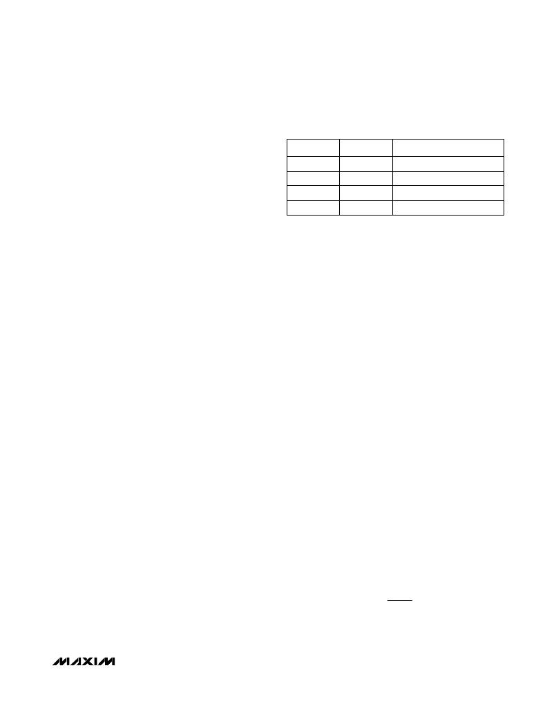
�Table� 2.� On/Off� Logic� Control�
�tion.� If� this� is� not� acceptable,� the� chip� should� be� held� in�
�shutdown� when� input� voltage� is� first� appled� to� ensure�
�that� the� linear� regulator� is� off� until� POUT� is� ready.�
�The� linear� regulator� in� the� MAX1705/MAX1706� features�
�a� 0.5� ?� ,� p-channel� MOSFET� pass� transistor.� This� pro-�
�vides� several� advantages,� including� longer� battery� life,�
�over� similar� designs� using� a� pnp� pass� transistor.� The� p-�
�ONA�
�0�
�0�
�1�
�1�
�ONB�
�0�
�1�
�0�
�1�
�MAX1705/MAX1706�
�On�
�Off�
�On�
�On�
�channel� MOSFET� requires� no� base-drive� current,� which�
�reduces� quiescent� current� considerably.� PNP-based�
�regulators� tend� to� waste� base-drive� current� in� dropout�
�when� the� pass� transistor� saturates.� The�
�MAX1705/MAX1706� eliminate� this� problem.�
�The� linear-regulator� error� amplifier� compares� the� output�
�feedback� sensed� at� the� FBLDO� input� against� the� inter-�
�nal� 1.250V� reference,� and� amplifies� the� difference�
�(Figure� 1).� The� MOSFET� driver� reads� the� error� signal�
�and� applies� the� appropriate� drive� to� the� p-channel�
�pass� transistor.� If� the� feedback� signal� is� lower� than� the�
�reference,� the� pass-transistor� gate� is� pulled� lower,�
�allowing� more� current� to� pass� to� the� output,� thereby�
�increasing� the� output� voltage.� If� the� feedback� voltage� is�
�too� high,� the� pass-transistor� gate� is� pulled� up,� allowing�
�less� current� to� pass� to� the� output.� Additional� blocks�
�include� a� current-limiting� block� and� a� thermal-overload�
�protection� block.�
�Low-Voltage� Startup� Oscillator�
�The� MAX1705/MAX1706� use� a� CMOS,� low-voltage� start-�
�up� oscillator� for� a� 1.1V� guaranteed� minimum� startup�
�input� voltage� at� +25°C.� On� startup,� the� low-voltage� oscil-�
�lator� switches� the� n-channel� MOSFET� until� the� output�
�voltage� reaches� 2.15V.� Above� this� level,� the� normal� step-�
�up� converter� feedback� and� control� circuitry� take� over.�
�Once� the� device� is� in� regulation,� it� can� operate� down� to� a�
�0.7V� input,� since� internal� power� for� the� IC� is� boot-�
�strapped� from� the� output� using� the� OUT� pin.�
�To� reduce� current� loading� during� step-up,� the� linear�
�regulator� is� kept� off� until� the� startup� converter� goes� into�
�regulation.� Minimum� startup� voltage� is� influenced� by�
�load� and� temperature� (see� the� Typical� Operating�
�Characteristics� ).� To� allow� proper� startup,� do� not� apply�
�a� full� load� at� POUT� until� after� the� device� has� exited�
�startup� mode� and� entered� normal� operation.�
�Shutdown�
�below� the� input,� but� the� linear� regulator� output� is�
�turned� off.�
�Entry� into� shutdown� mode� is� controlled� by� logic� input�
�pins� ONA� and� ONB� (Table� 2).� Both� inputs� have� trip�
�points� near� 0.5V� OUT� with� 0.15V� OUT� hysteresis.�
�Tracking�
�Connecting� TRACK� to� the� step-up� converter� output�
�implements� a� tracking� mode� that� sets� the� step-up�
�converter� output� to� 300mV� above� the� linear-regulator�
�output,� improving� efficiency.� In� track� mode,� feedback�
�for� the� step-up� converter� is� derived� from� the� OUT� pin.�
�When� TRACK� is� low,� the� step-up� converter� and� linear�
�regulator� are� separately� controlled� by� their� respective�
�feedback� inputs,� FB� and� FBLDO.� TRACK� is� a� logic�
�input� with� a� 0.5V� OUT� threshold,� and� should� be� hard-�
�wired� or� switched� with� a� slew� rate� exceeding� 1V/μs.�
�V� LDO� must� be� set� above� 2.3V� for� track� mode� to� operate�
�properly.�
�On� power-up� with� TRACK� =� OUT,� the� step-up� convert-�
�er� initially� uses� the� FB� input� to� regulate� its� output.� After�
�the� step-up� converter� goes� into� regulation� for� the� first�
�time,� the� linear� regulator� turns� on.� When� the� linear� regu-�
�lator� reaches� 2.3V,� track� mode� is� enabled� and� the� step-�
�up� converter� is� regulated� to� 300mV� above� the� linear-�
�regulator� output.�
�Low-Battery� Comparator�
�The� internal� low-battery� comparator� has� uncommitted�
�inputs� and� an� open-drain� output� capable� of� sinking�
�1mA.� To� use� it� as� a� low-battery-detection� comparator,�
�connect� the� LBN� input� to� the� reference,� and� connect�
�the� LBP� input� to� an� external� resistor-divider� between�
�the� positive� battery� terminal� and� GND� (Figure� 2).� The�
�resistor� values� are� then� as� follows:�
�R� 5� =� R� 6� ?�
�-� 1� ?�
�The� MAX1705/MAX1706� feature� a� shutdown� mode� that�
�reduces� quiescent� current� to� less� than� 1μA,� preserving�
�battery� life� when� the� system� is� not� in� use.� During� shut-�
�down,� the� reference,� the� low-battery� comparator,� and�
�?� V� IN,TH�
�?� V� LBN�
�?�
�?�
�all� feedback� and� control� circuitry� are� off.� The� step-up�
�converter’s� output� drops� to� one� Schottky� diode� drop�
�where� V� IN,TH� is� the� desired� input� voltage� trip� point� and�
�V� LBN� =� V� REF� =� 1.25V.� Since� the� input� bias� current� into�
�______________________________________________________________________________________�
�13�
�相关PDF资料 |
PDF描述 |
|---|---|
| URS1E221MPD | CAP ALUM 220UF 25V 20% RADIAL |
| URS1C331MPD | CAP ALUM 330UF 16V 20% RADIAL |
| URS1A471MPD | CAP ALUM 470UF 10V 20% RADIAL |
| RBM36DCAH | CONN EDGECARD 72POS R/A .156 SLD |
| RBM36DCAD | CONN EDGECARD 72POS R/A .156 SLD |
相关代理商/技术参数 |
参数描述 |
|---|---|
| MAX1705ESE+ | 制造商:Maxim Integrated Products 功能描述:1 TO 3-CELL HIGH-CURRENT LOW-NOIS - Rail/Tube |
| MAX1705EVKIT | 功能描述:直流/直流开关转换器 Evaluation Kit for the MAX1705 MAX1706 RoHS:否 制造商:STMicroelectronics 最大输入电压:4.5 V 开关频率:1.5 MHz 输出电压:4.6 V 输出电流:250 mA 输出端数量:2 最大工作温度:+ 85 C 安装风格:SMD/SMT |
| MAX17061AETI+ | 功能描述:LED照明驱动器 8-String White LED Driver w/SMBus RoHS:否 制造商:STMicroelectronics 输入电压:11.5 V to 23 V 工作频率: 最大电源电流:1.7 mA 输出电流: 最大工作温度: 安装风格:SMD/SMT 封装 / 箱体:SO-16N |
| MAX17061AETI+T | 功能描述:LED照明驱动器 8-String White LED Driver w/SMBus RoHS:否 制造商:STMicroelectronics 输入电压:11.5 V to 23 V 工作频率: 最大电源电流:1.7 mA 输出电流: 最大工作温度: 安装风格:SMD/SMT 封装 / 箱体:SO-16N |
| MAX17061AEVCMAXQU+ | 功能描述:LED 照明开发工具 Evaluation Kit/Evaluation system for MAX17061A RoHS:否 制造商:Fairchild Semiconductor 产品:Evaluation Kits 用于:FL7732 核心: 电源电压:120V 系列: 封装: |
发布紧急采购,3分钟左右您将得到回复。