- 您现在的位置:买卖IC网 > PDF目录13546 > MAX1763EEE+T (Maxim Integrated Products)IC REG BST SYNC 3.3V/ADJ 16QSOP PDF资料下载
参数资料
| 型号: | MAX1763EEE+T |
| 厂商: | Maxim Integrated Products |
| 文件页数: | 11/18页 |
| 文件大小: | 0K |
| 描述: | IC REG BST SYNC 3.3V/ADJ 16QSOP |
| 产品培训模块: | Lead (SnPb) Finish for COTS Obsolescence Mitigation Program |
| 标准包装: | 2,500 |
| 类型: | 升压(升压) |
| 输出类型: | 两者兼有 |
| 输出数: | 1 |
| 输出电压: | 3.3V,2.5 V ~ 5.5 V |
| 输入电压: | 0.7 V ~ 5.5 V |
| PWM 型: | 混合物 |
| 频率 - 开关: | 1MHz |
| 电流 - 输出: | 1.5A |
| 同步整流器: | 是 |
| 工作温度: | -40°C ~ 85°C |
| 安装类型: | 表面贴装 |
| 封装/外壳: | 16-SSOP(0.154",3.90mm 宽) |
| 包装: | 带卷 (TR) |
| 供应商设备封装: | 16-QSOP |
�� �
�
�1.5A,� Low-Noise,� 1MHz,� Step-Up�
�DC-DC� Converter�
�Table� 3.� On/Off� Logic� Control�
�ONA�
�0�
�ONB�
�0�
�MAX1763�
�On�
�R� G�
�20k�
�0�
�1�
�1�
�0�
�Off�
�On�
�V� IN�
�1.5� μ� H�
�C1�
�47� μ� F�
�2.5V�
�C� OUT�
�47� μ� F�
�1�
�1�
�On�
�AO�
�CLK/SEL�
�LX�
�3.3V�
�TO� V� IN� OR�
�V� OUT�
�POUT�
�ONB�
�POUT�
�MBRO520L�
�C4�
�220� μ� F�
�R3�
�AIN�
�MAX1763�
�AO�
�R6�
�150k�
�POWER-OK�
�OUTPUT�
�R3�
�165k�
�MAX1763�
�ONA� OUT�
�AIN�
�R5�
�4.7� Ω�
�C2�
�1� μ� F�
�R4�
�R4�
�100k�
�ISET�
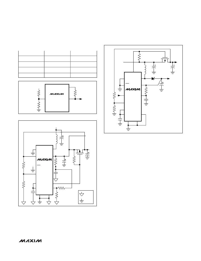
�Figure� 3.� Using� the� Gain� Block� as� a� Power-OK� Comparator�
�V� IN�
�C3�
�0.22� μ� F�
�REF�
�PGND�
�FB�
�GND�
�1.8V� TO� 5.5V�
�L1�
�1.5� μ� H�
�C1�
�47� μ� F�
�BOOST�
�OUTPUT�
�LINEAR-�
�Figure� 5.� Powering� a� Gain-Block� Linear� Regulator� from� the�
�Input� Voltage�
�CLK/SEL�
�LX�
�P�
�REGULATED�
�OUTPUT�
�stage� is� 10mS.� The� internal� gain� block� amplifies� the� dif-�
�ference� between� AIN� and� the� internal� 0.938V� reference.�
�R3�
�ONA� POUT�
�MAX1763�
�ONB� OUT�
�R5�
�4.7� Ω�
�C4�
�220� μ� F�
�R� G�
�20k�
�C� OUT�
�47� μ� F�
�To� provide� a� power-OK� signal,� connect� the� gain-block�
�input,� AIN,� to� an� external� resistor-divider� (Figure� 3).� The�
�input� bias� current� into� AIN� is� less� than� 30nA,� allowing�
�large-value� divider� resistors� without� sacrificing� accura-�
�cy.� Connect� the� resistor� voltage-divider� as� close� to� the�
�AIN�
�C2�
�1.0� μ� F�
�IC� as� possible,� within� 0.2in� (5mm)� of� AIN.� Choose� an�
�R4� value� of� 270k� Ω� or� less,� then� calculate� R3� using:�
�R3� =� R4((V� TRIP� /� V� AIN� )� -� 1)�
�R4�
�0.22� μ� F�
�ISET�
�REF�
�PGND�
�AO�
�FB�
�GND�
�R1�
�R2�
�30k�
�SIGNAL�
�GROUND�
�POWER�
�GROUND�
�where� V� AIN� is� 0.938V.�
�Figures� 4� and� 5� show� the� gain� block� used� in� a� linear-�
�regulator� application.� The� output� of� an� external� P-chan-�
�nel� pass� element� is� compared� to� an� internal� 0.938V�
�reference.� The� difference� is� amplified� and� drives� the�
�Figure� 4.� Using� the� Gain� Block� as� a� Linear� Regulator� from� the�
�Boosted� Output� Voltage�
�using� an� external� P-channel� MOSFET� pass� device.� The�
�gain-block� output� is� a� single-stage� transconductance�
�amplifier� that� drives� an� open-drain� N-channel� MOSFET.�
�The� transconductance� (G� M� )� of� the� entire� gain-block�
�gate� of� the� pass� element.� Use� a� logic-level� PFET,� such�
�as� Fairchild’s� NDS336P� (R� DS(ON)� =� 270m� Ω� ).� When� the�
�linear-regulator� output� voltage� is� in� regulation,� the�
�MOSFET� will� not� be� full� on;� thus,� the� on-resistance� will�
�not� be� important.� However,� if� the� linear� regulator� is� used�
�in� dropout,� the� MOSFET� on-resistance� will� determine�
�the� dropout� voltage� (V� DROPOUT� =� I� OUT� ?� R� DS(ON)� ).� If� a�
�lower� R� DS(ON)� PFET� is� used,� increase� the� linear-regula-�
�tor� output� filter� capacitance� to� maintain� stability.�
�______________________________________________________________________________________�
�11�
�相关PDF资料 |
PDF描述 |
|---|---|
| UUR1H330MCL6GS | CAP ALUM 33UF 50V 20% SMD |
| MAX6734KASYD3+T | IC SUPERVISOR MPU W/WD SOT23-8 |
| MAX1572ETC250+ | IC REG BUCK SYNC 2.5V .8A 12TQFN |
| MAX6734AKAVDD3+T | IC SUPERVISOR MPU W/WD SOT23-8 |
| MAX1701EEE+T | IC REG BST SYNC ADJ 0.8A 16QSOP |
相关代理商/技术参数 |
参数描述 |
|---|---|
| MAX1763EUE | 功能描述:直流/直流开关转换器 1.5A Low-Noise 1MHz Step-Up RoHS:否 制造商:STMicroelectronics 最大输入电压:4.5 V 开关频率:1.5 MHz 输出电压:4.6 V 输出电流:250 mA 输出端数量:2 最大工作温度:+ 85 C 安装风格:SMD/SMT |
| MAX1763EUE+ | 功能描述:直流/直流开关转换器 1.5A Low-Noise 1MHz Step-Up RoHS:否 制造商:STMicroelectronics 最大输入电压:4.5 V 开关频率:1.5 MHz 输出电压:4.6 V 输出电流:250 mA 输出端数量:2 最大工作温度:+ 85 C 安装风格:SMD/SMT |
| MAX1763EUE+T | 功能描述:直流/直流开关转换器 1.5A Low-Noise 1MHz Step-Up RoHS:否 制造商:STMicroelectronics 最大输入电压:4.5 V 开关频率:1.5 MHz 输出电压:4.6 V 输出电流:250 mA 输出端数量:2 最大工作温度:+ 85 C 安装风格:SMD/SMT |
| MAX1763EUE+TG069 | 制造商:Maxim Integrated Products 功能描述: |
| MAX1763EUE-T | 功能描述:直流/直流开关转换器 1.5A Low-Noise 1MHz Step-Up RoHS:否 制造商:STMicroelectronics 最大输入电压:4.5 V 开关频率:1.5 MHz 输出电压:4.6 V 输出电流:250 mA 输出端数量:2 最大工作温度:+ 85 C 安装风格:SMD/SMT |
发布紧急采购,3分钟左右您将得到回复。