- 您现在的位置:买卖IC网 > PDF目录20674 > MAX1765EEE+ (Maxim Integrated)IC REG DL BST/LINEAR SYNC 16QSOP PDF资料下载
参数资料
| 型号: | MAX1765EEE+ |
| 厂商: | Maxim Integrated |
| 文件页数: | 12/19页 |
| 文件大小: | 867K |
| 描述: | IC REG DL BST/LINEAR SYNC 16QSOP |
| 产品培训模块: | Lead (SnPb) Finish for COTS Obsolescence Mitigation Program |
| 标准包装: | 100 |
| 拓扑: | 升压(升压)同步(1),线性(LDO)(1) |
| 功能: | 任何功能 |
| 输出数: | 2 |
| 频率 - 开关: | 1MHz |
| 电压/电流 - 输出 1: | 2.5 V ~ 5.5 V,800mA |
| 电压/电流 - 输出 2: | 2.85V/可调,500mA |
| 带 LED 驱动器: | 无 |
| 带监控器: | 无 |
| 带序列发生器: | 无 |
| 电源电压: | 0.7 V ~ 5.5 V |
| 工作温度: | -40°C ~ 85°C |
| 安装类型: | 表面贴装 |
| 封装/外壳: | 16-SSOP(0.154",3.90mm 宽) |
| 供应商设备封装: | 16-QSOP |
| 包装: | 管件 |
PWM Operation in Normal Mode
The MAX1765 transitions to fixed-frequency PWM oper-
ation under medium and heavy loads. The N-channel
FET is engaged when V
FB
< V
REF
and is kept on to
ramp up the current in the inductor until one of the fol-
lowing conditions occurs: the system needs are met,
the next falling edge of the internal oscillator is
achieved, or the maximum inductor current (ISET) is
reached. The N-channel is turned off, activating the P-
channel synchronous rectifier that remains on until the
inductor current gets to the P-channel turn-off current
level, or V
FB
< V
REF
and there is a rising oscillator
clock edge. The 1MHz fixed-frequency operation pro-
duces an easily filtered fixed-noise spectrum.
Forced PWM Operation
When CLK/SEL is high, the MAX1765 operates in a low-
noise PWM-only mode. The N-channel FET is turned on
when V
FB
< V
REF
and is kept on to ramp up the induc-
tor current until one of the following conditions occurs:
the system needs are met, the next falling edge of the
internal oscillator is achieved, or the ISET is reached.
The N-channel is then turned off, activating the P-chan-
nel synchronous rectifier that remains on until the next
rising edge of the oscillator, where the N-channel is
again turned on under most conditions. The P-channel
zero detect circuitry is deactivated in forced PWM
mode. This means an N- or P-channel FET is on all the
time for most load conditions.
At light loads, the P-channel will remain on so the
device can pass current back to the input from the out-
put. The P-channel will only pass current for two cycles
before it is disabled. Then, the device remains inactive
until V
FB
< V
REF
.
During forced PWM operation, the MAX1765 switches
at a constant frequency (1MHz) and modulates the
MOSFET switch pulse width to control the power trans-
ferred per cycle in order to regulate the output voltage
for most output currents. Switching harmonics generat-
ed by fixed-frequency operation are consistent and
easily filtered. (See the Boost Followed by LDO Output
Noise Spectrum plot in the Typical Operating
Characteristics.)
Synchronized PWM Operation
The MAX1765 can be synchronized in PWM mode to
an external frequency of 500kHz to 1.2MHz by applying
an external clock signal to CLK/SEL. This allows inter-
ference to be minimized in wireless applications. The
synchronous rectifier is active during synchronized
PWM operation.
Synchronous Rectifier
The MAX1765 features an internal 250m? P-channel
synchronous rectifier to enhance efficiency. Synchronous
rectification provides a 5% efficiency improvement over
similar nonsynchronous boost regulators. In PWM mode,
the synchronous rectifier is turned on during the second
portion of each switching cycle. At light loads (in normal
mode), an internal comparator turns on the synchronous
rectifier when the voltage at LX exceeds the boost regu-
lator output, and turns it off when the inductor current
drops below 50mA.
Low-Voltage Startup Oscillator
The MAX1765 uses a low-voltage startup oscillator for a
1.1V guaranteed minimum input startup input voltage.
A Schottky diode placed across LX and POUT reduces
the startup voltage to 0.9V. At startup, the low-voltage
oscillator switches the N-channel MOSFET until the out-
put voltage reaches 2.15V. Above this level, the normal
boost-converter feedback and control circuitry takes
over. Once the device is in regulation, it can operate
down to 0.7V input since internal power for the IC is
bootstrapped from the OUT pin. Do not apply full load
until the output exceeds 2.3V.
800mA, Low-Noise, Step-Up DC-DC Converter
with 500mA Linear Regulator
12 ______________________________________________________________________________________
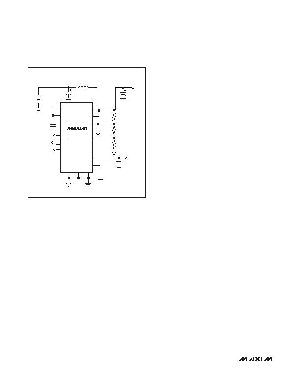
Figure 2. Typical Application Circuit
CLK/SELPGND
GND
ONL
TRACK
ONB
4.7糉
FBL
OUTL
33糉
3.3糎
REF
ILIM
4.7?/DIV>
LX
POUT
OUT
FB
LOGIC INPUTS
0.22糉
100糉
0.68糉
0.7V to 3.2V
MAX1765
ONA
V
IN
V
OUTL
=
2.85V
100k
165k
V
OUT
3.3V
INL
相关PDF资料 |
PDF描述 |
|---|---|
| GBB09DHFN | CONN CARDEDGE 18POS .050" SMD |
| EL7252CSZ-T7 | IC DRIVER MOSFET DUAL HS 8-SOIC |
| VI-J4X-CX-F3 | CONVERTER MOD DC/DC 5.2V 75W |
| ISL9104IRUFEVAL1Z | EVAL BOARD 1 FOR ISL9104IRUF |
| MAX4210EETT+T | IC CURRENT MONITOR 1.5% 6TDFN |
相关代理商/技术参数 |
参数描述 |
|---|---|
| MAX1765EEE+ | 功能描述:直流/直流开关转换器 800mA Step-Up w/500mA Linear Reg RoHS:否 制造商:STMicroelectronics 最大输入电压:4.5 V 开关频率:1.5 MHz 输出电压:4.6 V 输出电流:250 mA 输出端数量:2 最大工作温度:+ 85 C 安装风格:SMD/SMT |
| MAX1765EEE+T | 功能描述:直流/直流开关转换器 800mA Step-Up w/500mA Linear Reg RoHS:否 制造商:STMicroelectronics 最大输入电压:4.5 V 开关频率:1.5 MHz 输出电压:4.6 V 输出电流:250 mA 输出端数量:2 最大工作温度:+ 85 C 安装风格:SMD/SMT |
| MAX1765EEE-T | 功能描述:直流/直流开关转换器 800mA Step-Up w/500mA Linear Reg RoHS:否 制造商:STMicroelectronics 最大输入电压:4.5 V 开关频率:1.5 MHz 输出电压:4.6 V 输出电流:250 mA 输出端数量:2 最大工作温度:+ 85 C 安装风格:SMD/SMT |
| MAX1765EUE | 功能描述:直流/直流开关转换器 800mA Step-Up w/500mA Linear Reg RoHS:否 制造商:STMicroelectronics 最大输入电压:4.5 V 开关频率:1.5 MHz 输出电压:4.6 V 输出电流:250 mA 输出端数量:2 最大工作温度:+ 85 C 安装风格:SMD/SMT |
| MAX1765EUE+ | 功能描述:直流/直流开关转换器 800mA Step-Up w/500mA Linear Reg RoHS:否 制造商:STMicroelectronics 最大输入电压:4.5 V 开关频率:1.5 MHz 输出电压:4.6 V 输出电流:250 mA 输出端数量:2 最大工作温度:+ 85 C 安装风格:SMD/SMT |
发布紧急采购,3分钟左右您将得到回复。