- 您现在的位置:买卖IC网 > PDF目录20674 > MAX1765EEE+ (Maxim Integrated)IC REG DL BST/LINEAR SYNC 16QSOP PDF资料下载
参数资料
| 型号: | MAX1765EEE+ |
| 厂商: | Maxim Integrated |
| 文件页数: | 9/19页 |
| 文件大小: | 867K |
| 描述: | IC REG DL BST/LINEAR SYNC 16QSOP |
| 产品培训模块: | Lead (SnPb) Finish for COTS Obsolescence Mitigation Program |
| 标准包装: | 100 |
| 拓扑: | 升压(升压)同步(1),线性(LDO)(1) |
| 功能: | 任何功能 |
| 输出数: | 2 |
| 频率 - 开关: | 1MHz |
| 电压/电流 - 输出 1: | 2.5 V ~ 5.5 V,800mA |
| 电压/电流 - 输出 2: | 2.85V/可调,500mA |
| 带 LED 驱动器: | 无 |
| 带监控器: | 无 |
| 带序列发生器: | 无 |
| 电源电压: | 0.7 V ~ 5.5 V |
| 工作温度: | -40°C ~ 85°C |
| 安装类型: | 表面贴装 |
| 封装/外壳: | 16-SSOP(0.154",3.90mm 宽) |
| 供应商设备封装: | 16-QSOP |
| 包装: | 管件 |
800mA, Low-Noise, Step-Up DC-DC Converter
with 500mA Linear Regulator
_______________________________________________________________________________________ 9
PIN NAME
FUNCTION
1
FBL
Low-Dropout Linear Regulator Dual-Mode Feedback Input. Connect FBL to ground for 2.85V nominal
output voltage. Connect FBL to a resistor-divider from OUTL to ground for an adjustable output voltage.
FBL regulates to 1.25V.
2
ISET
Set N-Channel Current Limit. For maximum current limit, connect ISET to REF. To reduce current limit,
use a resistor-divider from REF to GND. If soft-start is desired, a capacitor can be added from ISET to
GND. When ONA = LO and ONB = HI or V
REF
< 80% of nominal value, an on-chip 100k?switchable
resistor discharges ISET to GND.
3
REF
1.25V Reference Output. Connect a 0.22礔 bypass capacitor to GND; 50礎 of external load current is
allowed. The reference is enabled if ONA = HI, ONB = LO, or ONL = HI.
4
GND Ground. Connect to PGND with short trace.
5
FB
Boost Converter Feedback Input. Connect a resistor-divider between OUT and GND to set the output
voltage in the range of 2.5V to 5V. In track mode, FB is disabled after OUTL is in regulation.
6
OUT
Boost Converter IC power is derived from OUT. Connect OUT to POUT through a 4.7?resistor and
bypass to GND with a 0.68礔 capacitor.
7
ONA ON Input. When high, the DC-DC is operational (Table 2).
8 CLK/SEL
CLOCK Input for the DC-DC Converter. Also serves to program operating mode of switch as follows:
CLK/SEL = LOW: Normal mode. Operates at a fixed frequency, automatically switching to low-power
(SKIP) mode when the load is minimized.
CLK/SEL = HI: Forced PWM mode. Operates in low-noise, constant-frequency mode at all loads.
CLK/SEL = Clocked: Synchronized forced PWM mode. The internal oscillator is synchronized to an
external clock in the 500kHz to 1200kHz frequency range.
Pin Description
0
0.4
0.2
0.8
0.6
1.2
1.0
1.4
0
0.4 0.6
0.2
0.8 1.0 1.2 1.4
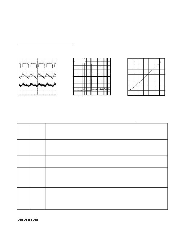
SWITCH CURRENT LIMIT vs. V
ISET
V
ISET
(V)
V
OUT
= +3.3
Typical Operating Characteristics (continued)
(T
A
= +25癈, unless otherwise noted.)
LIGHT-LOAD SWITCHING WAVEFORMS
(V
IN
= +2.4V, V
OUT
= +3.3V, I
OUT
= 10mA)
MAX1765 toc17
A: LX NODE, 5V/div
B: INDUCTOR CURRENT, 200mA/div, AC-COUPLED
C: OUTPUT RIPPLE, 20mV/div, AC-COUPLED
A
B
C
500ns/div
450
0.1
1
10
LINEAR-REGULATOR OUTPUT NOISE
50
0
FREQUENCY (MHz)
150
250
350
I
LDO
= 200mA
V
LDO
= 2.85V
相关PDF资料 |
PDF描述 |
|---|---|
| GBB09DHFN | CONN CARDEDGE 18POS .050" SMD |
| EL7252CSZ-T7 | IC DRIVER MOSFET DUAL HS 8-SOIC |
| VI-J4X-CX-F3 | CONVERTER MOD DC/DC 5.2V 75W |
| ISL9104IRUFEVAL1Z | EVAL BOARD 1 FOR ISL9104IRUF |
| MAX4210EETT+T | IC CURRENT MONITOR 1.5% 6TDFN |
相关代理商/技术参数 |
参数描述 |
|---|---|
| MAX1765EEE+ | 功能描述:直流/直流开关转换器 800mA Step-Up w/500mA Linear Reg RoHS:否 制造商:STMicroelectronics 最大输入电压:4.5 V 开关频率:1.5 MHz 输出电压:4.6 V 输出电流:250 mA 输出端数量:2 最大工作温度:+ 85 C 安装风格:SMD/SMT |
| MAX1765EEE+T | 功能描述:直流/直流开关转换器 800mA Step-Up w/500mA Linear Reg RoHS:否 制造商:STMicroelectronics 最大输入电压:4.5 V 开关频率:1.5 MHz 输出电压:4.6 V 输出电流:250 mA 输出端数量:2 最大工作温度:+ 85 C 安装风格:SMD/SMT |
| MAX1765EEE-T | 功能描述:直流/直流开关转换器 800mA Step-Up w/500mA Linear Reg RoHS:否 制造商:STMicroelectronics 最大输入电压:4.5 V 开关频率:1.5 MHz 输出电压:4.6 V 输出电流:250 mA 输出端数量:2 最大工作温度:+ 85 C 安装风格:SMD/SMT |
| MAX1765EUE | 功能描述:直流/直流开关转换器 800mA Step-Up w/500mA Linear Reg RoHS:否 制造商:STMicroelectronics 最大输入电压:4.5 V 开关频率:1.5 MHz 输出电压:4.6 V 输出电流:250 mA 输出端数量:2 最大工作温度:+ 85 C 安装风格:SMD/SMT |
| MAX1765EUE+ | 功能描述:直流/直流开关转换器 800mA Step-Up w/500mA Linear Reg RoHS:否 制造商:STMicroelectronics 最大输入电压:4.5 V 开关频率:1.5 MHz 输出电压:4.6 V 输出电流:250 mA 输出端数量:2 最大工作温度:+ 85 C 安装风格:SMD/SMT |
发布紧急采购,3分钟左右您将得到回复。