- 您现在的位置:买卖IC网 > PDF目录13148 > MAX1779EUE+ (Maxim Integrated Products)IC DC-DC CONV TRPL LCD 16-TSSOP PDF资料下载
参数资料
| 型号: | MAX1779EUE+ |
| 厂商: | Maxim Integrated Products |
| 文件页数: | 14/18页 |
| 文件大小: | 0K |
| 描述: | IC DC-DC CONV TRPL LCD 16-TSSOP |
| 产品培训模块: | Lead (SnPb) Finish for COTS Obsolescence Mitigation Program |
| 标准包装: | 96 |
| 应用: | 转换器,TFT,LCD |
| 输入电压: | 2.7 V ~ 5.5 V |
| 输出数: | 3 |
| 输出电压: | 2.7 V ~ 13 V |
| 工作温度: | 0°C ~ 85°C |
| 安装类型: | 表面贴装 |
| 封装/外壳: | 16-TSSOP(0.173",4.40mm 宽) |
| 供应商设备封装: | 16-TSSOP |
| 包装: | 管件 |
| 产品目录页面: | 1410 (CN2011-ZH PDF) |
�� �
�
�Low-Power� Triple-Output� TFT� LCD� DC-DC�
�Converter�
�nated� by� the� internal� switch� resistance� and� the� diode�
�impedance.� Start� with� 0.1μF� ceramic� capacitors.�
�Smaller� values� may� be� used� for� low-current� applica-�
�tions.�
�Charge-Pump� Output� Capacitor�
�Increasing� the� output� capacitance� or� decreasing� the�
�ESR� reduces� the� output� ripple� voltage� and� the� peak-to-�
�peak� transient� voltage.� Use� the� following� equation� to�
�approximate� the� required� capacitor� value:�
�C� PUMP� ≥� [I� PUMP� /� (125kHz� ?� V� RIPPLE� )]�
�Charge-Pump� Input� Capacitor�
�Use� a� bypass� capacitor� with� a� value� equal� to� or� greater�
�than� the� flying� capacitor.� Place� the� capacitor� as� close�
�to� the� IC� as� possible.� Connect� directly� to� PGND.�
�Rectifier� Diode�
�Use� Schottky� diodes� with� a� current� rating� equal� to� or�
�greater� than� 4� times� the� average� output� current,� and� a�
�voltage� rating� at� least� 1.5� times� V� SUPP� for� the� positive�
�charge� pump� and� V� SUPN� for� the� negative� charge� pump.�
�PC� Board� Layout� and� Grounding�
�Carefully� printed� circuit� layout� is� extremely� important� to�
�mum� load� current� that� the� LX� charge� pump� can� provide�
�and� is� limited� by� the� following� formula:�
�I� LXPUMP� =� ((N� +� 1)� ?� I� POS� )� +� (M� +� I� NEG� )� ≤� 5mA�
�where� N� is� the� number� of� stages� in� the� positive� low-�
�power� charge� pump,� and� M� is� the� number� of� stages� in�
�the� negative� charge� pump.� Applications� requiring� more�
�output� current� should� not� use� the� LX� charge� pump,� so�
�they� will� require� extra� stages� on� both� low-power� charge�
�pumps.� The� output� capacitor� of� this� unregulated�
�charge� pump� needs� to� be� stacked� on� top� of� the� main�
�output� in� order� to� keep� the� main� regulator� stable.�
�Increasing� the� integrator� capacitor� may� also� be�
�required� to� compensate� for� the� additional� charge-pump�
�capacitance� on� the� main� regulator� loop.�
�The� output� capacitor� of� this� unregulated� charge� pump�
�needs� to� be� stacked� on� top� of� the� main� output� in� order�
�to� keep� the� main� regulator� stable.� Increasing� the� inte-�
�grator� capacitor� may� also� be� required� to� compensate�
�for� the� additional� charge-pump� capacitance� on� the�
�main� regulator� loop.�
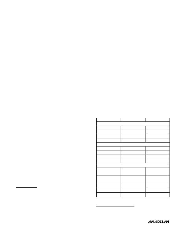
�Table� 1.� Component� Suppliers�
�minimize� ground� bounce� and� noise.� First,� place� the�
�main� boost� converter� output� diode� and� output� capacitor�
�less� than� 0.2in� (5mm)� from� the� LX� and� PGND� pins� with�
�wide� traces� and� no� vias.� Then� place� 0.1μF� ceramic�
�bypass� capacitors� near� the� charge-pump� input� pins�
�(SUPP� and� SUPN)� to� the� PGND� pin.� Keep� the� charge-�
�pump� circuitry� as� close� to� the� IC� as� possible,� using�
�wide� traces� and� avoiding� vias� when� possible.� Locate�
�all� feedback� resistive� dividers� as� close� to� their� respec-�
�tive� feedback� pins� as� possible.� The� PC� board� should�
�feature� separate� GND� and� PGND� areas� connected� at�
�only� one� point� under� the� IC.� To� maximize� output� power�
�and� efficiency� and� to� minimize� output� power� ripple� volt-�
�age,� use� extra� wide� power� ground� traces� and� solder�
�the� IC’s� power� ground� pin� directly� to� it.� Avoid� having�
�sensitive� traces� near� the� switching� nodes� and� high-cur-�
�rent� lines.�
�Refer� to� the� MAX1779� evaluation� kit� for� an� example� of�
�proper� board� layout.�
�Applications� Information�
�LX� Charge� Pump�
�Some� applications� require� multiple� charge-pump�
�SUPPLIER�
�INDUCTORS�
�Coilcraft�
�Coiltronics�
�Sumida� USA�
�Toko�
�CAPACITORS�
�AVX�
�Kemet�
�Sanyo�
�Taiyo� Yuden�
�DIODES�
�Central�
�Semiconductor�
�International�
�Rectifier�
�Motorola�
�Nihon�
�Zetex�
�PHONE�
�847-639-6400�
�561-241-7876�
�847-956-0666�
�847-297-0070�
�803-946-0690�
�408-986-0424�
�619-661-6835�
�408-573-4150�
�516-435-1110�
�310-322-3331�
�602-303-5454�
�847-843-7500�
�516-543-7100�
�FAX�
�847-639-1469�
�561-241-9339�
�847-956-0702�
�847-699-1194�
�803-626-3123�
�408-986-1442�
�619-661-1055�
�408-573-4159�
�516-435-1824�
�310-322-3332�
�602-994-6430�
�847-843-2798�
�516-864-7630�
�stages� due� to� low� supply� voltages.� In� order� to� reduce�
�the� circuit’s� size� and� component� count,� an� unregulated�
�charge� pump� may� be� added� onto� the� LX� switching�
�node.� The� configuration� shown� in� Figure� 4� works� well�
�for� most� applications.� The� maximum� output� current� of�
�the� low-power� charge� pumps� depends� on� the� maxi-�
�TRANSISTOR� COUNT:� 2846�
�Chip� Information�
�14�
�______________________________________________________________________________________�
�相关PDF资料 |
PDF描述 |
|---|---|
| RCC43DRTH-S93 | CONN EDGECARD 86POS DIP .100 SLD |
| ECC50DCMN-S288 | CONN EDGECARD 100POS .100 EXTEND |
| VE-B63-EU | CONVERTER MOD DC/DC 24V 200W |
| SPA221M0ER | CAP ALUM 220UF 2.5V 20% SMD |
| VI-J3K-EX-F1 | CONVERTER MOD DC/DC 40V 75W |
相关代理商/技术参数 |
参数描述 |
|---|---|
| MAX1779EUE+ | 功能描述:直流/直流开关转换器 Triple-Output TFT LCD RoHS:否 制造商:STMicroelectronics 最大输入电压:4.5 V 开关频率:1.5 MHz 输出电压:4.6 V 输出电流:250 mA 输出端数量:2 最大工作温度:+ 85 C 安装风格:SMD/SMT |
| MAX1779EUE+T | 功能描述:直流/直流开关转换器 Triple-Output TFT LCD RoHS:否 制造商:STMicroelectronics 最大输入电压:4.5 V 开关频率:1.5 MHz 输出电压:4.6 V 输出电流:250 mA 输出端数量:2 最大工作温度:+ 85 C 安装风格:SMD/SMT |
| MAX1779EUE-T | 功能描述:直流/直流开关转换器 RoHS:否 制造商:STMicroelectronics 最大输入电压:4.5 V 开关频率:1.5 MHz 输出电压:4.6 V 输出电流:250 mA 输出端数量:2 最大工作温度:+ 85 C 安装风格:SMD/SMT |
| MAX177C/D | 功能描述:模数转换器 - ADC RoHS:否 制造商:Texas Instruments 通道数量:2 结构:Sigma-Delta 转换速率:125 SPs to 8 KSPs 分辨率:24 bit 输入类型:Differential 信噪比:107 dB 接口类型:SPI 工作电源电压:1.7 V to 3.6 V, 2.7 V to 5.25 V 最大工作温度:+ 85 C 安装风格:SMD/SMT 封装 / 箱体:VQFN-32 |
| MAX177CNG | 功能描述:模数转换器 - ADC RoHS:否 制造商:Texas Instruments 通道数量:2 结构:Sigma-Delta 转换速率:125 SPs to 8 KSPs 分辨率:24 bit 输入类型:Differential 信噪比:107 dB 接口类型:SPI 工作电源电压:1.7 V to 3.6 V, 2.7 V to 5.25 V 最大工作温度:+ 85 C 安装风格:SMD/SMT 封装 / 箱体:VQFN-32 |
发布紧急采购,3分钟左右您将得到回复。