- 您现在的位置:买卖IC网 > PDF目录13148 > MAX1779EUE+ (Maxim Integrated Products)IC DC-DC CONV TRPL LCD 16-TSSOP PDF资料下载
参数资料
| 型号: | MAX1779EUE+ |
| 厂商: | Maxim Integrated Products |
| 文件页数: | 9/18页 |
| 文件大小: | 0K |
| 描述: | IC DC-DC CONV TRPL LCD 16-TSSOP |
| 产品培训模块: | Lead (SnPb) Finish for COTS Obsolescence Mitigation Program |
| 标准包装: | 96 |
| 应用: | 转换器,TFT,LCD |
| 输入电压: | 2.7 V ~ 5.5 V |
| 输出数: | 3 |
| 输出电压: | 2.7 V ~ 13 V |
| 工作温度: | 0°C ~ 85°C |
| 安装类型: | 表面贴装 |
| 封装/外壳: | 16-TSSOP(0.173",4.40mm 宽) |
| 供应商设备封装: | 16-TSSOP |
| 包装: | 管件 |
| 产品目录页面: | 1410 (CN2011-ZH PDF) |
�� �
�
�Low-Power� Triple-Output� TFT� LCD� DC-DC�
�Converter�
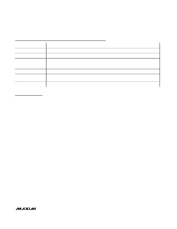
�Pin� Description� (continued)�
�PIN�
�10�
�11�
�12�
�13�
�14�
�15�
�16�
�NAME�
�DRVN�
�SUPN�
�DRVP�
�SUPP�
�PGND�
�LX�
�TGND�
�FUNCTION�
�Negative� Charge-Pump� Driver� Output.� Output� high� level� is� V� SUPN� ,� and� low� level� is� PGND.�
�Negative� Charge-Pump� Driver� Supply� Voltage.� Bypass� to� PGND� with� a� 0.1� μ� F� capacitor.�
�Positive� Charge-Pump� Driver� Output.� Output� high� level� is� V� SUPP� ,� and� low� level� is� PGND.�
�Positive� Charge-Pump� Driver� Supply� Voltage.� Bypass� to� PGND� with� a� 0.1� μ� F� capacitor.�
�Power� Ground.� Connect� to� GND� underneath� the� IC.�
�Main� Boost� Regulator� Power� MOSFET� N-Channel� Drain.� Connect� output� diode� and� output� capacitor�
�as� close� to� PGND� as� possible.�
�Must� be� connected� to� ground.�
�Detailed� Description�
�The� MAX1779� is� a� highly� efficient� triple-output� power�
�supply� for� TFT� LCD� applications.� The� device� contains�
�one� high-power� step-up� converter� and� two� low-power�
�charge� pumps.� The� primary� boost� converter� uses� an�
�internal� N-channel� MOSFET� to� provide� maximum� effi-�
�ciency� and� to� minimize� the� number� of� external� compo-�
�nents.� The� output� voltage� of� the� main� boost� converter�
�(V� MAIN� )� can� be� set� from� V� IN� to� 13V� with� external� resistors.�
�The� dual� charge� pumps� independently� regulate� a� posi-�
�tive� output� (V� POS� )� and� a� negative� output� (V� NEG� ).� These�
�low-power� outputs� use� external� diode� and� capacitor�
�stages� (as� many� stages� as� required)� to� regulate� output�
�voltages� up� to� +40V� and� down� to� -40V.� A� proprietary�
�regulation� algorithm� minimizes� output� ripple� as� well� as�
�capacitor� sizes� for� both� charge� pumps.�
�Also� included� in� the� MAX1779� are� a� precision� 1.25V�
�reference� that� sources� up� to� 50μA,� logic� shutdown,�
�soft-start,� power-up� sequencing,� fault� detection,� and� an�
�active-low� open-drain� ready� output.�
�Main� Boost� Converter�
�The� MAX1779� main� step-up� converter� switches� at� a�
�constant� 250kHz� internal� oscillator� frequency� to� allow�
�the� use� of� small� inductors� and� output� capacitors.� The�
�MOSFET� switch� pulse� width� is� modulated� to� control� the�
�power� transferred� on� each� switching� cycle� and� to� regu-�
�late� the� output� voltage.�
�During� PWM� operation,� the� internal� clock’s� rising� edge�
�sets� a� flip-flop,� which� turns� on� the� N-channel� MOSFET�
�(Figure� 1).� The� switch� turns� off� when� the� voltage-error,�
�slope-compensation,� and� current-feedback� signals� trip�
�the� comparators� and� reset� the� flip-flop.� The� switch�
�remains� off� for� the� rest� of� the� clock� cycle.� Changes� in�
�the� output� voltage� error� signal� shift� the� switch� current�
�trip� level,� consequently� modulating� the� MOSFET� duty�
�cycle.�
�Dual� Charge-Pump� Regulator�
�The� MAX1779� contains� two� individual� low-power� charge�
�pumps.� One� charge� pump� inverts� the� supply� voltage�
�(SUPN)� and� provides� a� regulated� negative� output� voltage.�
�The� second� charge� pump� doubles� the� supply� voltage�
�(SUPP)� and� provides� a� regulated� positive� output� voltage.�
�The� MAX1779� contains� internal� P-channel� and� N-channel�
�MOSFETs� to� control� the� power� transfer.� The� internal�
�MOSFETs� switch� at� a� constant� 125kHz� (0.5� ?� f� OSC� ).�
�Negative� Charge� Pump�
�During� the� first� half-cycle,� the� P-channel� MOSFET� turns�
�on� and� the� flying� capacitor� C5� charges� to� V� SUPN� minus�
�a� diode� drop� (Figure� 2).� During� the� second� half-cycle,�
�the� P-channel� MOSFET� turns� off,� and� the� N-channel�
�MOSFET� turns� on,� level� shifting� C5.� This� connects� C5� in�
�parallel� with� the� reservoir� capacitor� C6.� If� the� voltage�
�across� C6� minus� a� diode� drop� is� lower� than� the� voltage�
�across� C5,� charge� flows� from� C5� to� C6� until� the� diode�
�(D5)� turns� off.� The� amount� of� charge� transferred� to� the�
�output� is� controlled� by� the� variable� N-channel� on-resis-�
�tance.�
�Positive� Charge� Pump�
�During� the� first� half-cycle,� the� N-channel� MOSFET� turns�
�on� and� charges� the� flying� capacitor� C3� (Figure� 3).� This�
�initial� charge� is� controlled� by� the� variable� N-channel�
�on-resistance.� During� the� second� half-cycle,� the� N-�
�channel� MOSFET� turns� off� and� the� P-channel� MOSFET�
�turns� on,� level� shifting� C3� by� V� SUPP� volts.� This� connects�
�C3� in� parallel� with� the� reservoir� capacitor� C4.� If� the� volt-�
�age� across� C4� plus� a� diode� drop� (V� POS� +� V� DIODE� )� is�
�smaller� than� the� level-shifted� flying� capacitor� voltage�
�_______________________________________________________________________________________�
�9�
�相关PDF资料 |
PDF描述 |
|---|---|
| RCC43DRTH-S93 | CONN EDGECARD 86POS DIP .100 SLD |
| ECC50DCMN-S288 | CONN EDGECARD 100POS .100 EXTEND |
| VE-B63-EU | CONVERTER MOD DC/DC 24V 200W |
| SPA221M0ER | CAP ALUM 220UF 2.5V 20% SMD |
| VI-J3K-EX-F1 | CONVERTER MOD DC/DC 40V 75W |
相关代理商/技术参数 |
参数描述 |
|---|---|
| MAX1779EUE+ | 功能描述:直流/直流开关转换器 Triple-Output TFT LCD RoHS:否 制造商:STMicroelectronics 最大输入电压:4.5 V 开关频率:1.5 MHz 输出电压:4.6 V 输出电流:250 mA 输出端数量:2 最大工作温度:+ 85 C 安装风格:SMD/SMT |
| MAX1779EUE+T | 功能描述:直流/直流开关转换器 Triple-Output TFT LCD RoHS:否 制造商:STMicroelectronics 最大输入电压:4.5 V 开关频率:1.5 MHz 输出电压:4.6 V 输出电流:250 mA 输出端数量:2 最大工作温度:+ 85 C 安装风格:SMD/SMT |
| MAX1779EUE-T | 功能描述:直流/直流开关转换器 RoHS:否 制造商:STMicroelectronics 最大输入电压:4.5 V 开关频率:1.5 MHz 输出电压:4.6 V 输出电流:250 mA 输出端数量:2 最大工作温度:+ 85 C 安装风格:SMD/SMT |
| MAX177C/D | 功能描述:模数转换器 - ADC RoHS:否 制造商:Texas Instruments 通道数量:2 结构:Sigma-Delta 转换速率:125 SPs to 8 KSPs 分辨率:24 bit 输入类型:Differential 信噪比:107 dB 接口类型:SPI 工作电源电压:1.7 V to 3.6 V, 2.7 V to 5.25 V 最大工作温度:+ 85 C 安装风格:SMD/SMT 封装 / 箱体:VQFN-32 |
| MAX177CNG | 功能描述:模数转换器 - ADC RoHS:否 制造商:Texas Instruments 通道数量:2 结构:Sigma-Delta 转换速率:125 SPs to 8 KSPs 分辨率:24 bit 输入类型:Differential 信噪比:107 dB 接口类型:SPI 工作电源电压:1.7 V to 3.6 V, 2.7 V to 5.25 V 最大工作温度:+ 85 C 安装风格:SMD/SMT 封装 / 箱体:VQFN-32 |
发布紧急采购,3分钟左右您将得到回复。