- 您现在的位置:买卖IC网 > PDF目录1840 > MAX1791EUB+T (Maxim Integrated Products)IC REG CTRLR BUCK PWM CM 10-UMAX PDF资料下载
参数资料
| 型号: | MAX1791EUB+T |
| 厂商: | Maxim Integrated Products |
| 文件页数: | 18/20页 |
| 文件大小: | 0K |
| 描述: | IC REG CTRLR BUCK PWM CM 10-UMAX |
| 产品培训模块: | Lead (SnPb) Finish for COTS Obsolescence Mitigation Program |
| 标准包装: | 2,500 |
| PWM 型: | 电流模式 |
| 输出数: | 1 |
| 频率 - 最大: | 300kHz |
| 电源电压: | 5 V ~ 20 V |
| 降压: | 是 |
| 升压: | 无 |
| 回扫: | 无 |
| 反相: | 无 |
| 倍增器: | 无 |
| 除法器: | 无 |
| Cuk: | 无 |
| 隔离: | 无 |
| 工作温度: | -40°C ~ 85°C |
| 封装/外壳: | 10-TFSOP,10-MSOP(0.118",3.00mm 宽) |
| 包装: | 带卷 (TR) |
�� �
�
�High-Efficiency,� 10-Pin� μMAX,� Step-Down�
�Controllers� for� Notebooks�
�(Figure� 10).� Refer� to� the� MAX1791� EV� kit� manual� for� a�
�OUT�
�specific� layout� example.�
�FIXED�
�1.8V�
�FIXED�
�3.3V�
�TO� ERROR�
�AMP�
�If� possible,� mount� all� of� the� power� components� on� the�
�top� side� of� the� board,� with� their� ground� terminals� flush�
�against� one� another.� Follow� these� guidelines� for� good�
�PC� board� layout:�
�FB�
�?�
�Isolate� the� power� components� on� the� top� side� from�
�the� sensitive� analog� components� on� the� bottom�
�side� with� a� ground� shield.� Use� a� separate� GND�
�0.150V�
�2.5V�
�MAX1762�
�?�
�plane� under� OUT.� Avoid� the� introduction� of� AC� cur-�
�rents� into� the� GND� ground� planes.� Run� the� power�
�plane� ground� currents� on� the� top� side� only,� if� possi-�
�ble.�
�Keep� the� high-current� paths� short,� especially� at� the�
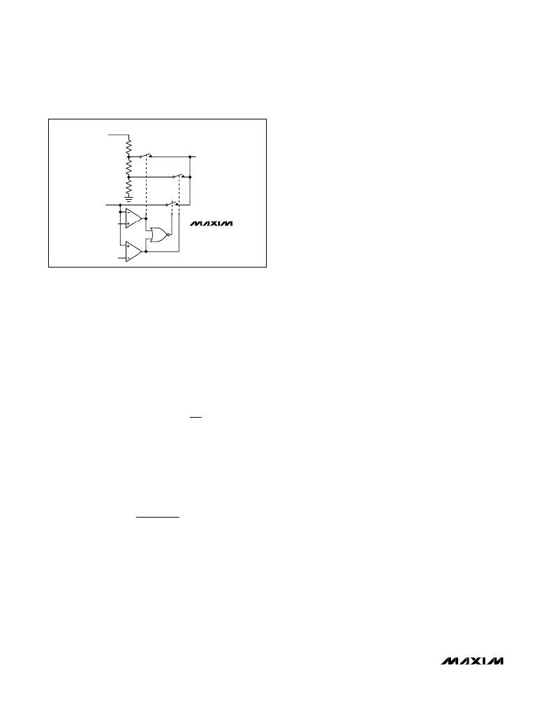
�Figure� 9.� Feedback� MUX�
�a� fixed� +1.8V� (MAX1762)� or� 3.3V� (MAX1791)� output.�
�Connect� FB� to� VL� for� a� fixed� 2.5V� (MAX1762)� or� 5.0V�
�(MAX1791)� output.� Otherwise,� connect� FB� to� a� resistive�
�voltage-divider� for� an� adjustable� output.�
�?�
�ground� terminals.� This� practice� is� essential� for� sta-�
�ble,� jitter-free� operation.�
�Keep� the� power� traces� and� load� connections� short.�
�This� practice� is� essential� for� high� efficiency.� Using�
�thick� copper� PC� boards� (2oz� vs.� 1oz)� can� enhance�
�full-load� efficiency� by� 1%� or� more.� Correctly� routing�
�PC� board� traces� is� a� difficult� task� that� must� be�
�Setting� the� Output� Voltage�
�Select� V� OUT� >� 1.25V� for� the� MAX1762/MAX1791� by�
�connecting� FB� to� a� resistive� voltage-divider� between�
�V� OUT� and� GND� (Figure� 2).� Choose� R2� to� be� about�
�10k� ?� ,� and� solve� for� R1� using� the� equation:�
�?�
�approached� in� terms� of� fractions� of� centimeters,�
�where� a� single� milliohm� of� excess� trace� resistance�
�causes� a� measurable� efficiency� penalty.�
�Inductor� and� GND� connections� to� the� synchronous�
�rectifiers� for� current� limiting� must� be� made� using�
�Kelvin� sensed� connections� to� guarantee� the� cur-�
�V� OUT� FB� � ?� 1� +�
�=� V� ?�
�?�
�?�
�?�
�R1� ?�
�R2� ?�
�rent-limit� accuracy.� With� 8-pin� SO� MOSFETs,� this� is�
�best� done� by� routing� power� to� the� MOSFETs� from�
�outside� using� the� top� copper� layer,� while� connect-�
�R2� =� ?� OUT� FB� ?� � R1�
�V� FB� REF� ?�
�?�
�where� V� FB� =� 1.25V.� For� a� V� OUT� =� 3.0V,� R2� =� 10k� ?� and�
�R1� =� 14k� ?� .�
�For� a� desired� V� OUT� <� 1.25V,� connect� FB� to� a� resistive�
�voltage-divider� between� REF� and� OUT� (Figure� 3).�
�Choose� R1� to� be� about� 50k� ?� ,� and� solve� for� R2� using�
�the� equation:�
�?� V� -V� ?�
�-V�
�where� V� FB� =� 1.25V� and� V� REF� =� 2.0V.� For� a� V� OUT� =�
�1.0V,� R1� =� 50k� ?� and� R2� =� 16.5k� ?� .� Under� these� condi-�
�tions,� a� minimum� load� of� V� REF� -� V� FB� /� R1� >15μA� is�
�required.�
�PC� Board� Layout� Guidelines�
�Careful� PC� board� layout� is� critical� to� achieve� low�
�switching� losses� and� clean,� stable� operation.� This� is�
�especially� true� when� multiple� converters� are� on� the�
�same� PC� board� where� one� circuit� can� affect� the� other.�
�The� switching� power� stages� require� particular� attention�
�?�
�?�
�?�
�ing� GND� and� CS� inside� (underneath)� the� μMAX�
�package.�
�When� trade-offs� in� trace� lengths� must� be� made,� it’s�
�preferable� to� allow� the� inductor� charging� path� to� be�
�made� longer� than� the� discharge� path.� For� example,�
�it’s� better� to� allow� some� extra� distance� between� the�
�input� capacitors� and� the� high-side� MOSFET� than� to�
�allow� distance� between� the� inductor� and� the� low-�
�side� MOSFET� or� between� the� inductor� and� the� out-�
�put� filter� capacitor.�
�Ensure� that� the� OUT� connection� to� C� OUT� is� short�
�and� direct.� However,� in� some� cases� it� may� be� desir-�
�able� to� deliberately� introduce� some� trace� length�
�between� the� OUT� connector� node� and� the� output�
�filter� capacitor� (see� Stability� Considerations� ).�
�Route� high-speed� switching� nodes� (CS,� DH,� and�
�DL)� away� from� sensitive� analog� areas� (FB).� Use�
�GND� as� an� EMI� shield� to� keep� radiated� switching�
�noise� away� from� the� IC’s� feedback� divider� and� ana-�
�log� bypass� capacitors.�
�18�
�______________________________________________________________________________________�
�相关PDF资料 |
PDF描述 |
|---|---|
| MAX1792EUA33+ | IC REG LDO 3.3V/ADJ .5A 8-UMAX |
| MAX1793EUE33+ | IC REG LDO 3.3V/ADJ 1A 16TSSOP |
| MAX1797EUA-T | IC REG BOOST SYNC FIX/ADJ 8UMAX |
| MAX1798EGP+T | IC POWER SUPPLY CDMA 20-QFN |
| MAX1801EKA+T | IC CNTRLR DC-DC SOT23-8 |
相关代理商/技术参数 |
参数描述 |
|---|---|
| MAX1791EVKIT | 功能描述:DC/DC 开关控制器 Evaluation Kit for the MAX1791 MAX1762 RoHS:否 制造商:Texas Instruments 输入电压:6 V to 100 V 开关频率: 输出电压:1.215 V to 80 V 输出电流:3.5 A 输出端数量:1 最大工作温度:+ 125 C 安装风格: 封装 / 箱体:CPAK |
| MAX1792EUA15 | 功能描述:低压差稳压器 - LDO 500mA RoHS:否 制造商:Texas Instruments 最大输入电压:36 V 输出电压:1.4 V to 20.5 V 回动电压(最大值):307 mV 输出电流:1 A 负载调节:0.3 % 输出端数量: 输出类型:Fixed 最大工作温度:+ 125 C 安装风格:SMD/SMT 封装 / 箱体:VQFN-20 |
| MAX1792EUA15+ | 功能描述:低压差稳压器 - LDO 500mA RoHS:否 制造商:Texas Instruments 最大输入电压:36 V 输出电压:1.4 V to 20.5 V 回动电压(最大值):307 mV 输出电流:1 A 负载调节:0.3 % 输出端数量: 输出类型:Fixed 最大工作温度:+ 125 C 安装风格:SMD/SMT 封装 / 箱体:VQFN-20 |
| MAX1792EUA15+T | 功能描述:低压差稳压器 - LDO 500mA RoHS:否 制造商:Texas Instruments 最大输入电压:36 V 输出电压:1.4 V to 20.5 V 回动电压(最大值):307 mV 输出电流:1 A 负载调节:0.3 % 输出端数量: 输出类型:Fixed 最大工作温度:+ 125 C 安装风格:SMD/SMT 封装 / 箱体:VQFN-20 |
| MAX1792EUA15-T | 功能描述:低压差稳压器 - LDO 500mA RoHS:否 制造商:Texas Instruments 最大输入电压:36 V 输出电压:1.4 V to 20.5 V 回动电压(最大值):307 mV 输出电流:1 A 负载调节:0.3 % 输出端数量: 输出类型:Fixed 最大工作温度:+ 125 C 安装风格:SMD/SMT 封装 / 箱体:VQFN-20 |
发布紧急采购,3分钟左右您将得到回复。