- 您现在的位置:买卖IC网 > PDF目录5055 > MAX1820XEUB+ (Maxim Integrated Products)IC REG BUCK WCDMA 10-MSOP PDF资料下载
参数资料
| 型号: | MAX1820XEUB+ |
| 厂商: | Maxim Integrated Products |
| 文件页数: | 15/18页 |
| 文件大小: | 0K |
| 描述: | IC REG BUCK WCDMA 10-MSOP |
| 产品培训模块: | Lead (SnPb) Finish for COTS Obsolescence Mitigation Program |
| 标准包装: | 50 |
| 应用: | 转换器,WCDMA 功率放大器应用 |
| 输入电压: | 2.6 V ~ 5.5 V |
| 输出数: | 1 |
| 输出电压: | 0.4 V ~ 3.4 V |
| 工作温度: | -40°C ~ 85°C |
| 安装类型: | 表面贴装 |
| 封装/外壳: | 10-TFSOP,10-MSOP(0.118",3.00mm 宽) |
| 供应商设备封装: | 10-µMAX |
| 包装: | 管件 |
�� �
�
�WCDMA� Cellular� Phone� 600mA�
�Buck� Regulators�
�Output� Capacitor� Selection�
�The� output� capacitor� is� required� to� keep� the� output� volt-�
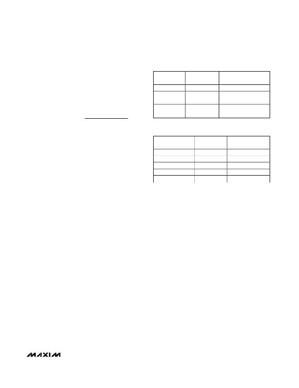
�Table� 2.� Capacitor� Selection�
�(� 2� � ?� OSC� � C� OUT� )� ?� ?�
�age� ripple� small� and� to� ensure� regulation� control� loop�
�stability.� The� output� capacitor� must� have� low� imped-�
�ance� at� the� switching� frequency.� Ceramic� capacitors�
�are� recommended.� The� output� ripple� is� approximately:�
�V� RIPPLE� ≈� LIR� ?� I� OUT(MAX)�
�?� 1� ?�
�� ?� ESR� +� ?�
�?� ?�
�CAPACITOR�
�C� BATT�
�C� OUT�
�(MAX1820)�
�C� OUT�
�(MAX1821)�
�CAPACITOR�
�VALUE� (μF)�
�4.7� to� 10�
�2.2� to� 4.7�
�4.7� to� 10�
�ESR�
�(m� ?� )�
�<150�
�<50�
�<150�
�CAPACITOR�
�TYPE�
�Ceramic�
�Ceramic�
�Ceramic�
�See� the� Compensation� Design� section� for� a� discussion�
�Table� 3.� Component� Manufacturers�
�of� the� influence� of� output� capacitance� and� ESR� on� reg-�
�ulation� control-loop� stability.�
�The� capacitor� voltage� rating� must� exceed� the� maximum�
�applied� capacitor� voltage.� Consult� the� manufacturer’s�
�specifications� for� proper� capacitor� derating.� Avoid� Y5V�
�and� Z5U� dielectric� types� due� to� their� huge� voltage� and�
�temperature� coefficients� of� capacitance� and� ESR.�
�PC� Board� Layout� and� Routing�
�MANUFACTURER�
�Coilcraft�
�Kemet�
�Panasonic�
�Sumida�
�Taiyo� Yuden�
�USA� PHONE�
�NUMBER�
�847-639-6400�
�408-986-0424�
�847-468-5624�
�847-956-0666�
�408-573-4150�
�WEBSITE�
�www.coilcraft.com�
�www.kemet.com�
�www.panasonic.com�
�www.sumida.com�
�www.t-yuden.com�
�High� switching� frequencies� and� large� peak� currents�
�make� PC� board� layout� a� very� important� part� of� design.�
�Good� design� minimizes� excessive� EMI� on� the� feedback�
�paths� and� voltage� gradients� in� the� ground� plane,� both�
�of� which� can� result� in� instability� or� regulation� errors.�
�Connect� the� inductor,� input� filter� capacitor,� and� output�
�filter� capacitor� as� close� together� as� possible,� and� keep�
�their� traces� short,� direct,� and� wide.� Connect� their�
�ground� pins� at� a� single� common� node� in� a� star-ground�
�configuration.� The� external� voltage-feedback� network�
�should� be� very� close� to� the� FB� pin,� within� 0.2in� (5mm).�
�Keep� noisy� traces� (from� the� LX� pin,� for� example)� away�
�from� the� voltage-feedback� network;� also,� keep� them�
�separate,� using� grounded� copper.� Connect� GND� and�
�PGND� at� a� single� point,� as� close� as� possible� to� the�
�MAX1820/MAX1821.� The� MAX1820/MAX1821� evalua-�
�tion� kit� manual� illustrates� an� example� PC� board� layout�
�and� routing� scheme.�
�UCSP� Package� Consideration�
�For� general� UCSP� package� information� and� PC� layout�
�considerations,� refer� to� the� Maxim� Application� Note�
�(Wafer-Level� Ultra-Chip-Board-Scale� Package).�
�______________________UCSP� Reliability�
�The� chip-scale� package� (UCSP)� represents� a� unique�
�packaging� form� factor� that� may� not� perform� equally� to� a�
�packaged� product� through� traditional� mechanical� relia-�
�bility� tests.� UCSP� reliability� is� integrally� linked� to� the�
�user’s� assembly� methods,� circuit� board� material,� and�
�usage� environment.� The� user� should� closely� review�
�these� areas� when� considering� use� of� a� UCSP� package.�
�Performance� through� Operating� Life� Test� and� Moisture�
�Resistance� remains� uncompromised� as� it� is� primarily�
�determined� by� the� wafer-fabrication� process.�
�Mechanical� stress� performance� is� a� greater� considera-�
�tion� for� a� UCSP� package.� UCSPs� are� attached� through�
�direct� solder� contact� to� the� user’s� PC� board,� foregoing�
�the� inherent� stress� relief� of� a� packaged-product� lead�
�frame.� Solder� joint� contact� integrity� must� be� consid-�
�ered.� Information� on� Maxim’s� qualification� plan,� test�
�data,� and� recommendations� are� detailed� in� the� UCSP�
�application� note,� which� can� be� found� on� Maxim’s� website,�
�www.maxim-ic.com.�
�____________________Chip� Information�
�TRANSISTOR� COUNT:� 2722�
�______________________________________________________________________________________�
�15�
�相关PDF资料 |
PDF描述 |
|---|---|
| EBA40DTKT | CONN EDGECARD 80POS DIP .125 SLD |
| P1330-223K | INDUCTOR POWER 22.0UH SMD |
| X5649S14-2.7 | IC SUPERVISOR CPU 64K EE 14-SOIC |
| EEV-HD1E470P | CAP ALUM 47UF 25V 20% SMD |
| ECA43DTKN | CONN EDGECARD 86POS DIP .125 SLD |
相关代理商/技术参数 |
参数描述 |
|---|---|
| MAX1820XEUB+ | 功能描述:直流/直流开关调节器 WCDMA 600mA Buck Regulator RoHS:否 制造商:International Rectifier 最大输入电压:21 V 开关频率:1.5 MHz 输出电压:0.5 V to 0.86 V 输出电流:4 A 输出端数量: 最大工作温度: 安装风格:SMD/SMT 封装 / 箱体:PQFN 4 x 5 |
| MAX1820XEUB+T | 功能描述:直流/直流开关调节器 WCDMA 600mA Buck Regulator RoHS:否 制造商:International Rectifier 最大输入电压:21 V 开关频率:1.5 MHz 输出电压:0.5 V to 0.86 V 输出电流:4 A 输出端数量: 最大工作温度: 安装风格:SMD/SMT 封装 / 箱体:PQFN 4 x 5 |
| MAX1820XEUB-T | 功能描述:直流/直流开关调节器 RoHS:否 制造商:International Rectifier 最大输入电压:21 V 开关频率:1.5 MHz 输出电压:0.5 V to 0.86 V 输出电流:4 A 输出端数量: 最大工作温度: 安装风格:SMD/SMT 封装 / 箱体:PQFN 4 x 5 |
| MAX1820YEBC | 制造商:Maxim Integrated Products 功能描述:WCDMA CELLULAR PHONE 600MA BUCK REG - Rail/Tube |
| MAX1820YEBC+ | 制造商:Maxim Integrated Products 功能描述:CONV DC-DC SGL-OUT STEP DOWN 12UCSP - Rail/Tube |
发布紧急采购,3分钟左右您将得到回复。