- 您现在的位置:买卖IC网 > PDF目录383338 > MAX1845ETX (MAXIM INTEGRATED PRODUCTS INC) Dual, High-Efficiency, Step-Down Controller with Accurate Current Limit PDF资料下载
参数资料
| 型号: | MAX1845ETX |
| 厂商: | MAXIM INTEGRATED PRODUCTS INC |
| 元件分类: | 稳压器 |
| 英文描述: | Dual, High-Efficiency, Step-Down Controller with Accurate Current Limit |
| 中文描述: | DUAL SWITCHING CONTROLLER, 620 kHz SWITCHING FREQ-MAX, QCC36 |
| 封装: | 6 X 6 MM, 0.80 MM, MO220WJJD-1, TQFN-36 |
| 文件页数: | 17/27页 |
| 文件大小: | 543K |
| 代理商: | MAX1845ETX |
第1页第2页第3页第4页第5页第6页第7页第8页第9页第10页第11页第12页第13页第14页第15页第16页当前第17页第18页第19页第20页第21页第22页第23页第24页第25页第26页第27页
M
Dual, High-Efficiency, Step-Down
Controller with Accurate Current Limit
______________________________________________________________________________________
17
The overvoltage trip level depends on the internal or
external output voltage feedback divider and is restrict-
ed by the output voltage adjustment range (1V to 5.5V)
and by the absolute maximum rating of OUT_. Setting
the overvoltage threshold higher than the output volt-
age adjustment range is not recommended.
Output Undervoltage Protection
The output voltage can be continuously monitored for
undervoltage. When undervoltage protection is
enabled (UVP = V
CC
), if the output is less than 70% of
the error-amplifier trip voltage, undervoltage protection
is triggered. If an overvoltage protection threshold is
set, the DL low-side gate driver is forced high. This
activates the low-side MOSFET switch, which rapidly
discharges the output capacitor, reduces the input
voltage, and grounds the outputs. If the overvoltage
protection is disabled (OVP = V
CC
) and an undervolt-
age event occurs, the gate drivers are turned off and
the outputs float. Connect UVP to GND to disable
undervoltage protection.
Note that DL latching high causes the output voltage to
dip slightly negative when energy has been previously
stored in the LC tank circuit. For loads that cannot tol-
erate a negative voltage, place a power Schottky diode
across the output to act as a reverse polarity clamp.
Also, note the nonstandard logic levels if actively dri-
ving UVP (see the
Electrical Characteristics
).
Design Procedure
Firmly establish the input voltage range and maximum
load current before choosing a switching frequency
and inductor operating point (ripple-current ratio). The
primary design trade-off lies in choosing a good
switching frequency and inductor operating point, and
the following four factors dictate the rest of the design:
1)
Input Voltage Range.
The maximum value
(V
IN(MAX)
) must accommodate the worst-case high
AC adapter voltage. The minimum value (V
IN(MIN)
)
must account for the lowest battery voltage after
drops due to connectors, fuses, and battery selector
switches. Lower input voltages result in better effi-
ciency.
2)
Maximum Load Current.
There are two values to
consider. The
peak load current
(I
LOAD(MAX)
) deter-
mines the instantaneous component stresses and
filtering requirements, and thus drives output capac-
itor selection, inductor saturation rating, and the
design of the current-limit circuit. The
continuous
load current
(I
LOAD
) determines the thermal stress-
es and thus drives the selection of input capacitors,
MOSFETs, and other critical heat-contributing com-
ponents.
3)
Switching Frequency.
This choice determines the
basic trade-off between size and efficiency. The
optimal frequency is largely a function of maximum
input voltage due to MOSFET switching losses that
are proportional to frequency and V
IN
2.
4)
Inductor Operating Point.
This choice provides
trade-offs between size vs. efficiency. Low inductor
values cause large ripple currents, resulting in the
smallest size, but poor efficiency and high output
noise. The minimum practical inductor value is one
that causes the circuit to operate at the edge of criti-
cal conduction (where the inductor current just
touches zero with every cycle at maximum load).
Inductor values lower than this grant no further size-
reduction benefit.
The MAX1845
’
s pulse-skipping algorithm initiates
skip mode at the critical conduction point. So, the
inductor operating point also determines the load-
current value at which PFM/PWM switchover occurs.
The optimum point is usually found between 20%
and 50% ripple current.
Inductor Selection
The switching frequency (on-time) and operating point
(% ripple or LIR) determine the inductor value as fol-
lows:
V
(V
V
f
LIR
IN
×
×
Example: I
LOAD(MAX)
= 8A, V
IN
= 15V, V
OUT
= 1.8V,
f = 300kHz, 25% ripple current or LIR = 0.25:
1.8V (15V - 1 8V)
15V
345kHz
×
×
L
0.25
8A
2.3 H
=
×
=
L =
- V
I
×
)
OUT
IN
OUT
LOAD(MAX)
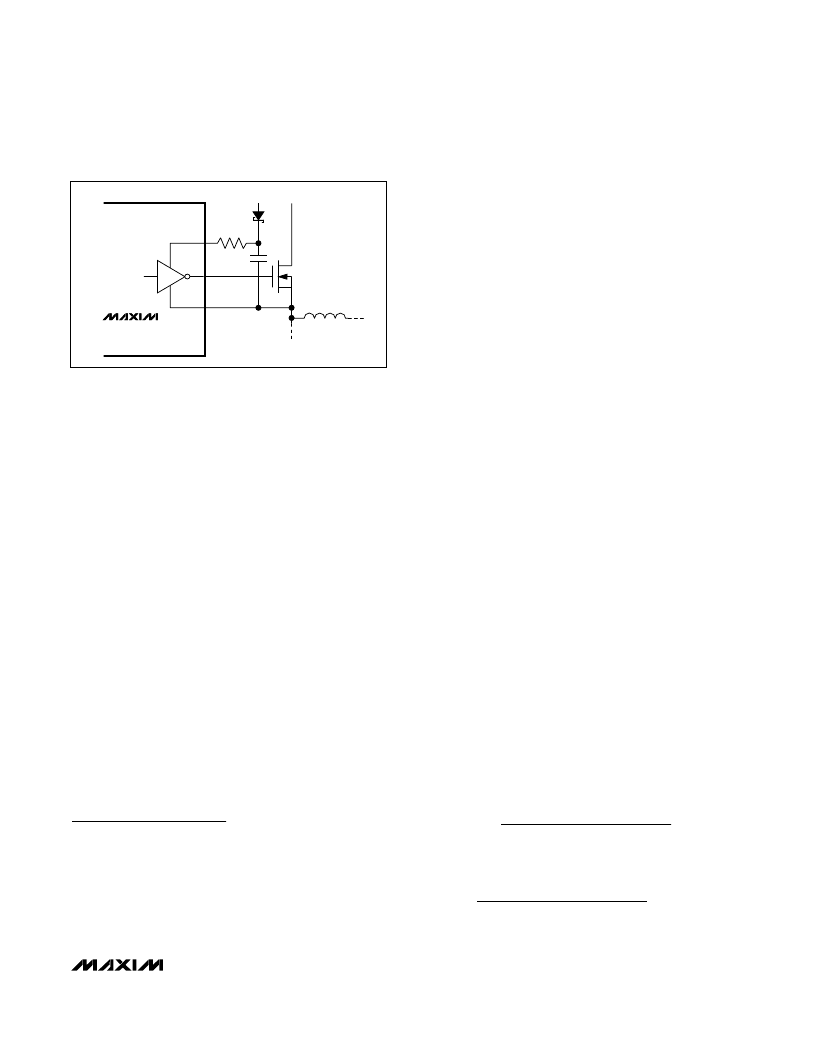
BST
+5V
V
IN
5
DH
LX
MAX1845
Figure 6. Reducing the Switching-Node Rise Time
相关PDF资料 |
PDF描述 |
|---|---|
| MAX1848 | Replaced by TMS320VC5506 : DSP (DSP Only) for Embedded V90 Modem Solution [Not Recommended For New Designs (NRND)] 144-LQFP |
| MAX1848ETA | Replaced by TMS320VC5506 : DSP (DSP Only) for Embedded V90 Modem Solution [Not Recommended For New Designs (NRND)] 144-BGA MICROSTAR |
| MAX1848EKA | White LED Step-Up Converter in SOT23 |
| MAX1855 | Fixed-Point Digital Signal Processor 352-FC/CSP 0 to 0 |
| MAX1854EEG | High-Speed, Adjustable, Synchronous Step-Down Controllers with Integrated Voltage Positioning |
相关代理商/技术参数 |
参数描述 |
|---|---|
| MAX1845ETX+ | 功能描述:电流型 PWM 控制器 Step-Down Controller RoHS:否 制造商:Texas Instruments 开关频率:27 KHz 上升时间: 下降时间: 工作电源电压:6 V to 15 V 工作电源电流:1.5 mA 输出端数量:1 最大工作温度:+ 105 C 安装风格:SMD/SMT 封装 / 箱体:TSSOP-14 |
| MAX1845ETX+T | 功能描述:电流型 PWM 控制器 Step-Down Controller RoHS:否 制造商:Texas Instruments 开关频率:27 KHz 上升时间: 下降时间: 工作电源电压:6 V to 15 V 工作电源电流:1.5 mA 输出端数量:1 最大工作温度:+ 105 C 安装风格:SMD/SMT 封装 / 箱体:TSSOP-14 |
| MAX1845ETX-T | 功能描述:电流型 PWM 控制器 RoHS:否 制造商:Texas Instruments 开关频率:27 KHz 上升时间: 下降时间: 工作电源电压:6 V to 15 V 工作电源电流:1.5 mA 输出端数量:1 最大工作温度:+ 105 C 安装风格:SMD/SMT 封装 / 箱体:TSSOP-14 |
| MAX1845ETX-TG068 | 制造商:Rochester Electronics LLC 功能描述: 制造商:Maxim Integrated Products 功能描述: |
| MAX1845EVKIT | 功能描述:电源管理IC开发工具 Evaluation Kit for the MAX1845 RoHS:否 制造商:Maxim Integrated 产品:Evaluation Kits 类型:Battery Management 工具用于评估:MAX17710GB 输入电压: 输出电压:1.8 V |
发布紧急采购,3分钟左右您将得到回复。