- 您现在的位置:买卖IC网 > PDF目录1841 > MAX1857EUA47+ (Maxim Integrated Products)IC REG LDO 4.75V/ADJ .5A 8-UMAX PDF资料下载
参数资料
| 型号: | MAX1857EUA47+ |
| 厂商: | Maxim Integrated Products |
| 文件页数: | 8/10页 |
| 文件大小: | 0K |
| 描述: | IC REG LDO 4.75V/ADJ .5A 8-UMAX |
| 产品培训模块: | Lead (SnPb) Finish for COTS Obsolescence Mitigation Program |
| 标准包装: | 50 |
| 稳压器拓扑结构: | 正,固定式或可调式 |
| 输出电压: | 4.75V,1.25 V ~ 5 V |
| 输入电压: | 2.5 V ~ 5.5 V |
| 稳压器数量: | 1 |
| 电流 - 输出: | 500mA(最小) |
| 工作温度: | -40°C ~ 85°C |
| 安装类型: | 表面贴装 |
| 封装/外壳: | 8-TSSOP,8-MSOP(0.118",3.00mm 宽) |
| 供应商设备封装: | 8-uMAX |
| 包装: | 管件 |
| 产品目录页面: | 1410 (CN2011-ZH PDF) |
�� �
�
�500mA,� Low-Dropout,�
�Ripple-Rejecting� LDO� in� μMAX�
�shut� down,� RST� is� held� low� independent� of� the� output�
�voltage.� If� unused,� leave� RST� grounded� or� unconnected.�
�Current� Limit�
�The� MAX1857� monitors� and� controls� the� pass� transis-�
�tor� ’� s� gate� voltage,� limiting� the� output� current� to� 1.2A.�
�This� current� limit� doubles� when� the� output� voltage� is�
�within� 4%� of� the� nominal� value� to� improve� performance�
�with� large� load� transients.� The� output� can� be� shorted� to�
�0.7�
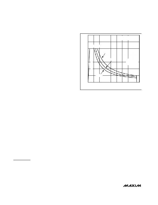
�0.6�
�0.5�
�0.4�
�CONTINUOUS� CURRENT� LIMIT�
�T� A� =� +50� °� C�
�μ� MAX� PACKAGE� OPERATING�
�REGION� AT� T� J(MAX)� =� +150� °� C�
�ground� for� an� indefinite� period� of� time� without� damag-�
�ing� the� part.�
�0.3�
�T� A� =� +70� °� C�
�MAXIMUM� SUPPLY�
�VOLTAGE� LIMIT�
�(V� OUT� =� 1.25V)�
�Thermal� Overload� Protection�
�Thermal� overload� protection� limits� total� power� dissipa-�
�tion� in� the� MAX1857.� When� the� junction� temperature�
�0.2�
�exceeds� T� J� =� +170� °� C,� a� thermal� sensor� turns� off� the�
�pass� transistor,� allowing� the� device� to� cool.� The� thermal�
�sensor� turns� the� pass� transistor� on� again� after� the� junc-�
�0.1�
�T� A� =� +85� °� C�
�tion� temperature� cools� by� 20� °� C,� resulting� in� a� pulsed�
�output� during� continuous� thermal� overload� conditions.�
�Thermal� overload� protection� protects� the� MAX1857� in�
�0�
�0�
�0.5�
�1.0�
�1.5� 2.0� 2.5� 3.0� 3.5�
�INPUT-OUTPUT� VOLTAGE� DIFFERENTIAL� (V)�
�4.0�
�4.5�
�the� event� of� fault� conditions.� For� continuous� operation,�
�do� not� exceed� the� absolute� maximum� junction-temper-�
�ature� rating� of� T� J� =� +150� °� C.�
�Operating� Region� and�
�Power� Dissipation�
�The� MAX1857� ’� s� maximum� power� dissipation� depends� on�
�the� thermal� resistance� of� the� IC� package� and� circuit�
�board,� the� temperature� difference� between� the� die� junc-�
�tion� and� ambient� air,� and� the� rate� of� air� flow.� The� power�
�dissipated� in� the� device� is� P� =� I� OUT� x� (V� IN� -� V� OUT� ).� The�
�maximum� allowed� power� dissipation� is� 330mW� or:�
�P� MAX� =� (T� J(MAX)� -� T� A� )� /� (� θ� JC� +� θ� CA� )�
�where� T� J� -� T� A� is� the� temperature� difference� between�
�the� MAX1857� die� junction� and� the� surrounding� air;� θ� JC�
�is� the� thermal� resistance� from� the� junction� to� the� case;�
�and� θ� CA� is� the� thermal� resistance� from� the� case�
�through� the� PC� board,� copper� traces,� and� other� materi-�
�als� to� the� surrounding� air.�
�The� MAX1857� delivers� up� to� 0.5A� RMS� and� operates� with�
�input� voltages� up� to� 5.5V,� but� not� simultaneously.� High�
�output� currents� can� only� be� sustained� when� input-output�
�differential� voltages� are� low,� as� shown� in� Figure� 3.�
�Applications� Information�
�Capacitor� Selection�
�and� Regulator� Stability�
�Capacitors� are� required� at� the� MAX1857� ’� s� input� and�
�output� for� stable� operation� over� the� full� temperature�
�range� and� with� load� currents� up� to� 500mA.� Connect� a�
�1μF� capacitor� between� IN� and� ground� and� a� 3.3μF� low�
�Figure� 3.� Power� Operating� Regions:� Maximum� Output� Current�
�vs.� Supply� Voltage�
�equivalent� series� resistance� (ESR)� capacitor� between�
�OUT� and� ground.� For� output� voltages� less� than� 2V,� use�
�a� 4.7μF� low-ESR� output� capacitor.� The� input� capacitor�
�(C� IN� )� lowers� the� source� impedance� of� the� input� supply.�
�Reduce� noise� and� improve� load-transient� response,�
�stability,� and� power-supply� rejection� by� using� larger�
�output� capacitors� such� as� 10μF.�
�The� output� capacitor� ’� s� (C� OUT� )� ESR� affects� stability� and�
�output� noise.� Use� output� capacitors� with� an� ESR� of�
�0.1� ?� or� less� to� ensure� stability� and� optimum� transient�
�response.� Surface-mount� ceramic� capacitors� have� very�
�low� ESR� and� are� commonly� available� in� values� up� to�
�10μF.� Connect� C� IN� and� C� OUT� as� close� to� the� MAX1857�
�as� possible� to� minimize� the� impact� of� PC� board� trace�
�inductance.�
�Noise,� PSRR,� and� Transient� Response�
�The� MAX1857� is� designed� to� operate� with� low� dropout�
�voltages� and� low� quiescent� currents� in� battery-powered�
�systems� while� still� maintaining� good� noise,� transient�
�response,� and� AC� rejection.� See� the� Typical� Operating�
�Characteristics� for� a� plot� of� power-supply� rejection� ratio�
�(PSRR)� vs.� frequency.� When� operating� from� noisy�
�sources,� improved� supply-noise� rejection� and� transient�
�response� can� be� achieved� by� increasing� the� values� of�
�the� input� and� output� bypass� capacitors� and� through�
�passive� filtering� techniques.�
�The� MAX1857� load-transient� response� graphs� (see�
�Typical� Operating� Characteristics� )� show� two� compo-�
�8�
�_______________________________________________________________________________________�
�相关PDF资料 |
PDF描述 |
|---|---|
| MAX1858EEG+T | IC REG CTRLR BUCK PWM VM 24-QSOP |
| MAX1865TEEP+T | IC PWR SUPPLY CONTROLLER 20QSOP |
| MAX1873REEE+T | IC CNTRLR CHARGE LI+ 16-QSOP |
| MAX1874ETE+ | IC LI+ CHARGER DUAL-IN 16-TQFN |
| MAX1875AEEG+ | IC REG CTRLR BUCK PWM VM 24-QSOP |
相关代理商/技术参数 |
参数描述 |
|---|---|
| MAX1857EUA47+ | 功能描述:低压差稳压器 - LDO 500mA Ripple-Rejecting RoHS:否 制造商:Texas Instruments 最大输入电压:36 V 输出电压:1.4 V to 20.5 V 回动电压(最大值):307 mV 输出电流:1 A 负载调节:0.3 % 输出端数量: 输出类型:Fixed 最大工作温度:+ 125 C 安装风格:SMD/SMT 封装 / 箱体:VQFN-20 |
| MAX1857EUA47+T | 功能描述:低压差稳压器 - LDO 500mA Ripple-Rejecting RoHS:否 制造商:Texas Instruments 最大输入电压:36 V 输出电压:1.4 V to 20.5 V 回动电压(最大值):307 mV 输出电流:1 A 负载调节:0.3 % 输出端数量: 输出类型:Fixed 最大工作温度:+ 125 C 安装风格:SMD/SMT 封装 / 箱体:VQFN-20 |
| MAX1857EUA47-T | 功能描述:低压差稳压器 - LDO 500mA Ripple-Rejecting RoHS:否 制造商:Texas Instruments 最大输入电压:36 V 输出电压:1.4 V to 20.5 V 回动电压(最大值):307 mV 输出电流:1 A 负载调节:0.3 % 输出端数量: 输出类型:Fixed 最大工作温度:+ 125 C 安装风格:SMD/SMT 封装 / 箱体:VQFN-20 |
| MAX1858AEEG | 功能描述:DC/DC 开关控制器 RoHS:否 制造商:Texas Instruments 输入电压:6 V to 100 V 开关频率: 输出电压:1.215 V to 80 V 输出电流:3.5 A 输出端数量:1 最大工作温度:+ 125 C 安装风格: 封装 / 箱体:CPAK |
| MAX1858AEEG+ | 功能描述:电压模式 PWM 控制器 Dual 180 Out Buck Controllers RoHS:否 制造商:Texas Instruments 输出端数量:1 拓扑结构:Buck 输出电压:34 V 输出电流: 开关频率: 工作电源电压:4.5 V to 5.5 V 电源电流:600 uA 最大工作温度:+ 125 C 最小工作温度:- 40 C 封装 / 箱体:WSON-8 封装:Reel |
发布紧急采购,3分钟左右您将得到回复。