- 您现在的位置:买卖IC网 > PDF目录383338 > MAX186ACWP (MAXIM INTEGRATED PRODUCTS INC) Low-Power, 8-Channel, Serial 12-Bit ADCs PDF资料下载
参数资料
| 型号: | MAX186ACWP |
| 厂商: | MAXIM INTEGRATED PRODUCTS INC |
| 元件分类: | ADC |
| 英文描述: | Low-Power, 8-Channel, Serial 12-Bit ADCs |
| 中文描述: | 8-CH 12-BIT SUCCESSIVE APPROXIMATION ADC, SERIAL ACCESS, PDSO20 |
| 封装: | SO-20 |
| 文件页数: | 7/24页 |
| 文件大小: | 245K |
| 代理商: | MAX186ACWP |
Digital Ground
Positive Supply Voltage, +5V ±5%
M
Low-Power, 8-Channel,
S erial 12-Bit ADCs
_______________________________________________________________________________________
7
PIN
NAME
FUNCTION
12
REFADJ
13
AGND
Analog Ground. Also IN- Input for single-ended conversions.
14
DGND
15
DOUT
Serial Data Output. Data is clocked out at the falling edge of SCLK. High impedance when
CS
is high.
16
SSTRB
17
DIN
18
CS
19
SCLK
Input to the Reference-Buffer Amplifier. To disable the reference-buffer amplifier, tie REFADJ to
V
DD
.
Serial Clock Input. Clocks data in and out of serial interface. In external clock mode, SCLK also sets
the conversion speed. (Duty cycle must be 40% to 60% in external clock mode.)
Serial Strobe Output. In internal clock mode, SSTRB goes low when the MAX186/MAX188 begin the
A/D conversion and goes high when the conversion is done. In external clock mode, SSTRB pulses
high for one clock period before the MSB decision. High impedance when
CS
is high (external mode).
Active-Low Chip Select. Data will not be clocked into DIN unless
CS
is low. When
CS
is high, DOUT
is high impedance.
Serial Data Input. Data is clocked in at the rising edge of SCLK.
20
V
DD
+5V
3k
C
LOAD
DGND
DOUT
C
LOAD
DGND
3k
DOUT
a. High-Z to V
OH
and V
OL
to V
OH
b. High-Z to V
OL
and V
OH
to V
OL
+5V
3k
C
LOAD
DGND
DOUT
C
LOAD
DGND
3k
DOUT
a V
OH
to High-Z
b V
OL
to High-Z
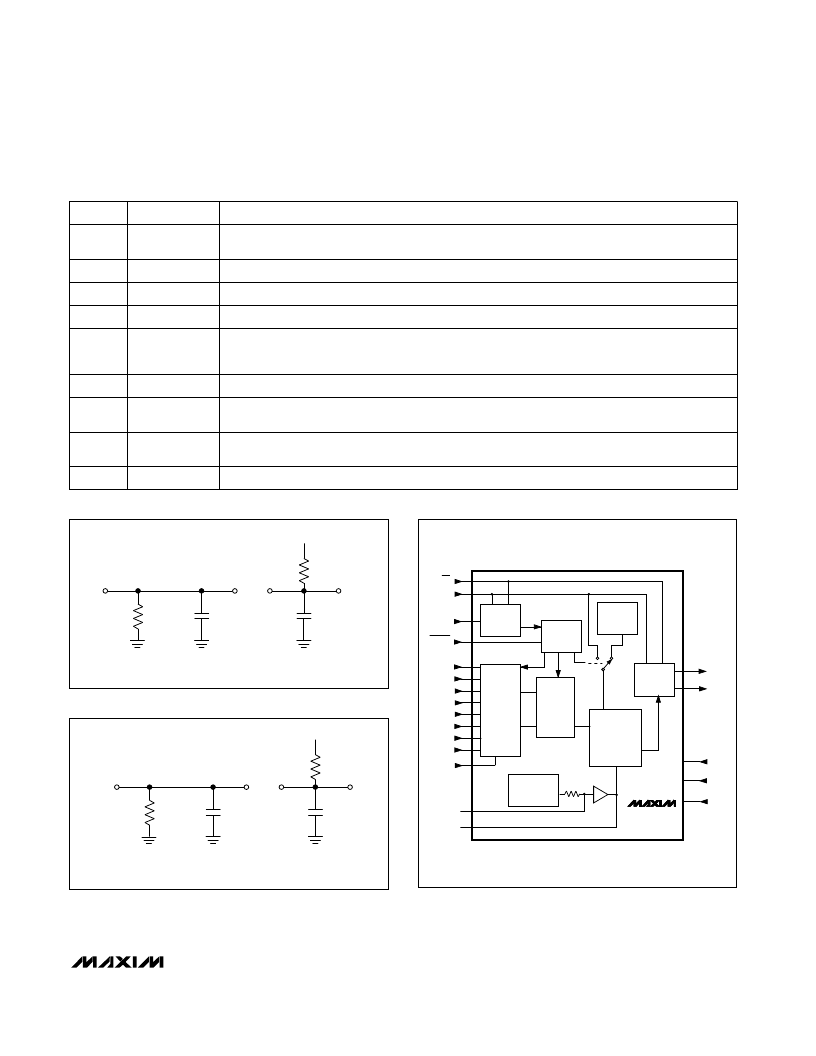
Figure 1. Load Circuits for Enable Time
Figure 2. Load Circuits for Disabled Time
INPUT
SHIFT
REGISTER
CONTROL
LOGIC
INT
CLOCK
OUTPUT
SHIFT
REGISTER
+2.46V
REFERENCE
(MAX186)
T/H
ANALOG
INPUT
MUX
12-BIT
SAR
ADC
REF
IN
DOUT
SSTRB
V
DD
DGND
V
SS
SCLK
DIN
CH0
CH1
CH2
CH3
CH4
CH7
CH6
CH5
AGND
REFADJ
VREF
OUT
CLOCK
+4.096V
20k
≈
1.65
1
2
3
4
5
6
7
8
10
11
12
13
15
16
17
18
19
MAX186
MAX188
CS
SHDN
A
20
14
9
Figure 3. Block Diagram
________________________________________________Pin Desc ription (c ontinued)
相关PDF资料 |
PDF描述 |
|---|---|
| MAX186CCAP | Low-Power, 8-Channel, Serial 12-Bit ADCs |
| MAX186BCPP | Low-Power, 8-Channel, Serial 12-Bit ADCs |
| MAX186DEAP | Low-Power, 8-Channel, Serial 12-Bit ADCs |
| MAX186BCAP | Low-Power, 8-Channel, Serial 12-Bit ADCs |
| MAX186BCWP | Low-Power, 8-Channel, Serial 12-Bit ADCs |
相关代理商/技术参数 |
参数描述 |
|---|---|
| MAX186ACWP+ | 功能描述:模数转换器 - ADC 12-Bit 8Ch 133ksps 5.25V Precision ADC RoHS:否 制造商:Texas Instruments 通道数量:2 结构:Sigma-Delta 转换速率:125 SPs to 8 KSPs 分辨率:24 bit 输入类型:Differential 信噪比:107 dB 接口类型:SPI 工作电源电压:1.7 V to 3.6 V, 2.7 V to 5.25 V 最大工作温度:+ 85 C 安装风格:SMD/SMT 封装 / 箱体:VQFN-32 |
| MAX186ACWP+T | 功能描述:模数转换器 - ADC 12-Bit 8Ch 133ksps 5.25V Precision ADC RoHS:否 制造商:Texas Instruments 通道数量:2 结构:Sigma-Delta 转换速率:125 SPs to 8 KSPs 分辨率:24 bit 输入类型:Differential 信噪比:107 dB 接口类型:SPI 工作电源电压:1.7 V to 3.6 V, 2.7 V to 5.25 V 最大工作温度:+ 85 C 安装风格:SMD/SMT 封装 / 箱体:VQFN-32 |
| MAX186ACWP-T | 功能描述:模数转换器 - ADC RoHS:否 制造商:Texas Instruments 通道数量:2 结构:Sigma-Delta 转换速率:125 SPs to 8 KSPs 分辨率:24 bit 输入类型:Differential 信噪比:107 dB 接口类型:SPI 工作电源电压:1.7 V to 3.6 V, 2.7 V to 5.25 V 最大工作温度:+ 85 C 安装风格:SMD/SMT 封装 / 箱体:VQFN-32 |
| MAX186AEAP | 功能描述:模数转换器 - ADC RoHS:否 制造商:Texas Instruments 通道数量:2 结构:Sigma-Delta 转换速率:125 SPs to 8 KSPs 分辨率:24 bit 输入类型:Differential 信噪比:107 dB 接口类型:SPI 工作电源电压:1.7 V to 3.6 V, 2.7 V to 5.25 V 最大工作温度:+ 85 C 安装风格:SMD/SMT 封装 / 箱体:VQFN-32 |
| MAX186AEAP+ | 功能描述:模数转换器 - ADC 12-Bit 8Ch 133ksps 5.25V Precision ADC RoHS:否 制造商:Texas Instruments 通道数量:2 结构:Sigma-Delta 转换速率:125 SPs to 8 KSPs 分辨率:24 bit 输入类型:Differential 信噪比:107 dB 接口类型:SPI 工作电源电压:1.7 V to 3.6 V, 2.7 V to 5.25 V 最大工作温度:+ 85 C 安装风格:SMD/SMT 封装 / 箱体:VQFN-32 |
发布紧急采购,3分钟左右您将得到回复。