- 您现在的位置:买卖IC网 > PDF目录5139 > MAX1880EUG+T (Maxim Integrated Products)IC DC-DC CONV QUAD LCD 24TSSOP PDF资料下载
参数资料
| 型号: | MAX1880EUG+T |
| 厂商: | Maxim Integrated Products |
| 文件页数: | 21/39页 |
| 文件大小: | 0K |
| 描述: | IC DC-DC CONV QUAD LCD 24TSSOP |
| 产品培训模块: | Lead (SnPb) Finish for COTS Obsolescence Mitigation Program |
| 标准包装: | 2,500 |
| 应用: | 转换器,TFT,LCD |
| 输入电压: | 2.7 V ~ 5.5 V |
| 输出数: | 4 |
| 输出电压: | 2.7 V ~ 13 V |
| 工作温度: | 0°C ~ 85°C |
| 安装类型: | 表面贴装 |
| 封装/外壳: | 24-TSSOP(0.173",4.40mm 宽) |
| 供应商设备封装: | 24-TSSOP |
| 包装: | 带卷 (TR) |
第1页第2页第3页第4页第5页第6页第7页第8页第9页第10页第11页第12页第13页第14页第15页第16页第17页第18页第19页第20页当前第21页第22页第23页第24页第25页第26页第27页第28页第29页第30页第31页第32页第33页第34页第35页第36页第37页第38页第39页
�� �
�
�MAX1778/MAX1880–MAX1885�
�Quad-Output� TFT� LCD� DC/DC�
�Converters� with� Buffer�
�The� switching� waveforms� appear� noisy� and� asynchro-�
�nous� when� light� loading� causes� pulse-skipping� opera-�
�tion;� this� is� a� normal� operating� condition� that� improves�
�light-load� efficiency.�
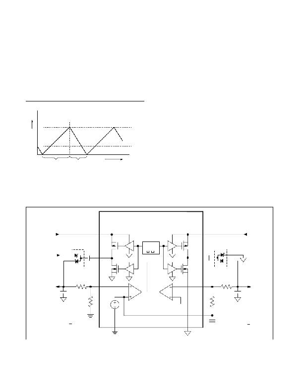
�Dual� Charge-Pump� Regulator� (MAX1778/�
�MAX1880–MAX1882� Only)�
�The� MAX1778/MAX1880–MAX1882� controllers� contain�
�two� independent� low-power� charge� pumps� (Figure� 4).�
�One� charge� pump� inverts� the� input� voltage� and� pro-�
�vides� a� regulated� negative� output� voltage.� The� second�
�charge� pump� doubles� the� input� voltage� and� provides� a�
�regulated� positive� output� voltage.� The� controllers�
�contain� internal� p-channel� and� n-channel� MOSFETs� to�
�control� the� power� transfer.� The� internal� MOSFETs�
�switch� at� a� constant� frequency� (fCHP� =� fOSC/2).�
�I� PEAK�
�Positive� Charge� Pump�
�During� the� first� half-cycle,� the� n-channel� MOSFET� turns�
�TIME�
�I� LOAD�
�on� and� charges� flying� capacitor� C� X(POS)� (Figure� 4).�
�This� initial� charge� is� controlled� by� the� variable�
�n-channel� on-resistance.� During� the� second� half-cycle,�
�the� n-channel� MOSFET� turns� off� and� the� p-channel�
�t� ON�
�t� OFF�
�MOSFET� turns� on,� level� shifting� C� X(POS)� by� V� SUPP� volts.�
�This� connects� C� X(POS)� in� parallel� with� the� reservoir�
�capacitor� C� OUT(POS)� .� If� the� voltage� across� C� OUT(POS)�
�plus� a� diode� drop� (V� POS� +� V� DIODE� )� is� smaller� than� the�
�Figure� 3.� Discontinuous-to-Continuous� Conduction� Crossover�
�Point�
�level-shifted� flying� capacitor� voltage� (V� CX(POS)� +�
�V� SUPP� ),� charge� flows� from� C� X(POS)� to� C� OUT(POS)� until�
�the� diode� (D3)� turns� off.�
�MAX1778�
�MAX1880�
�MAX1881�
�V� SUPP�
�SUPP�
�MAX1882�
�SUPN�
�V� SUPN�
�2.7V� TO� 13V�
�OSC�
�2.7V� TO� 13V�
�V� SUPD�
�D2�
�C� X(POS)�
�DRVP�
�DRVN�
�C� X(NEG)�
�D4�
�D3�
�D5�
�V� POS�
�R3�
�FBP�
�FBN�
�R5�
�V� NEG�
�C� OUT(POS)�
�C� OUT(NEG)�
�R4�
�V� REF�
�1.25V�
�REF�
�R6�
�1� R3�
�V� POS� =� (� +� R4� )� V� REF�
�GND�
�PGND�
�C� REF�
�0.22� μ� F�
�R5�
�V� NEG� =� -� (� R6� )� V� REF�
�V� REF� =� 1.25V�
�Figure� 4.� Low-Power� Charge� Pump� Block� Diagram�
�Maxim� Integrated�
�V� REF� =� 1.25V�
�21�
�相关PDF资料 |
PDF描述 |
|---|---|
| X40420V14I-B | IC VOLT MON DUAL SUP/SW 14-TSSOP |
| SIP21106DR-30-E3 | IC REG LDO 3V .15A SC70-5 |
| X40420V14I-AT1 | IC VOLT MON DUAL SUP/SW 14-TSSOP |
| 200USC2200MEFCSN35X45 | CAP ALUM 2200UF 200V 20% SNAP-IN |
| RMM25DRSN-S288 | CONN EDGECARD 50POS .156 EXTEND |
相关代理商/技术参数 |
参数描述 |
|---|---|
| MAX1881EUG | 功能描述:直流/直流开关转换器 RoHS:否 制造商:STMicroelectronics 最大输入电压:4.5 V 开关频率:1.5 MHz 输出电压:4.6 V 输出电流:250 mA 输出端数量:2 最大工作温度:+ 85 C 安装风格:SMD/SMT |
| MAX1881EUG+ | 功能描述:直流/直流开关转换器 Quad-Output TFT LCD RoHS:否 制造商:STMicroelectronics 最大输入电压:4.5 V 开关频率:1.5 MHz 输出电压:4.6 V 输出电流:250 mA 输出端数量:2 最大工作温度:+ 85 C 安装风格:SMD/SMT |
| MAX1881EUG+T | 功能描述:直流/直流开关转换器 Quad-Output TFT LCD RoHS:否 制造商:STMicroelectronics 最大输入电压:4.5 V 开关频率:1.5 MHz 输出电压:4.6 V 输出电流:250 mA 输出端数量:2 最大工作温度:+ 85 C 安装风格:SMD/SMT |
| MAX1881EUG-T | 功能描述:直流/直流开关转换器 RoHS:否 制造商:STMicroelectronics 最大输入电压:4.5 V 开关频率:1.5 MHz 输出电压:4.6 V 输出电流:250 mA 输出端数量:2 最大工作温度:+ 85 C 安装风格:SMD/SMT |
| MAX1882EUG | 功能描述:LCD 驱动器 Quad-Output TFT LCD DC-DC Converter with Buffer RoHS:否 制造商:Maxim Integrated 数位数量:4.5 片段数量:30 最大时钟频率:19 KHz 工作电源电压:3 V to 3.6 V 最大工作温度:+ 85 C 最小工作温度:- 20 C 封装 / 箱体:PDIP-40 封装:Tube |
发布紧急采购,3分钟左右您将得到回复。