- 您现在的位置:买卖IC网 > PDF目录9869 > MAX191ACWG+T (Maxim Integrated Products)IC ADC 12BIT 100KSPS 24-SOIC PDF资料下载
参数资料
| 型号: | MAX191ACWG+T |
| 厂商: | Maxim Integrated Products |
| 文件页数: | 11/24页 |
| 文件大小: | 0K |
| 描述: | IC ADC 12BIT 100KSPS 24-SOIC |
| 产品培训模块: | Lead (SnPb) Finish for COTS Obsolescence Mitigation Program |
| 标准包装: | 1,000 |
| 位数: | 12 |
| 采样率(每秒): | 100k |
| 数据接口: | MICROWIRE?,并联,QSPI?,串行,SPI? |
| 转换器数目: | 1 |
| 功率耗散(最大): | 941mW |
| 电压电源: | 双 ± |
| 工作温度: | 0°C ~ 70°C |
| 安装类型: | 表面贴装 |
| 封装/外壳: | 24-SOIC(0.295",7.50mm 宽) |
| 供应商设备封装: | 24-SOIC W |
| 包装: | 带卷 (TR) |
| 输入数目和类型: | 2 个单端,单极;2 个单端,双极;1 个差分,单极;1 个差分,双极 |
which can be achieved using power-down between
conversions.
External Compensation
Figure 19a shows the connection for external compensa-
tion with reference adjustment. In this mode, an external
4.7F capacitor compensates the reference output
amplifier, allowing for maximum conversion speed and
lowest conversion noise. However, when reactivating the
ADC after power-down, the reference takes typically 2ms
to fully charge the 4.7F capacitor, so more time is
required before a conversion can start (Figure 19b).
Thus, the average current consumed in power-up/power-
down operations is higher in external compensation
mode than in internal compensation mode.
Gain and Offset Adjustment
Figure 20 depicts the nominal, unipolar input/output (I/O)
transfer function, and Figure 22 shows the bipolar I/O
transfer function. Code transitions occur halfway between
successive integer LSB values. Note that 1LSB = 1.00mV
(4.096V/4096) for unipolar operation and 1LSB = 1.00mV
((4.096V/2 - -4.096V/2)/4096) for bipolar operation.
Figures 19a and 21a show how to adjust the ADC gain
in applications that require full-scale range adjustment.
The connection shown in Figure 21a provides ±0.5%
for ±20LSBs of adjustment range and is recommended
for applications that use an external reference. On the
other hand, Figure 19a is recommended for applica-
tions that use the internal reference, because it uses
fewer external components.
If both offset and full scale need adjustment, the circuit
in Figure 21b is recommended. For single-supply
ADCs, it is virtually impossible to null system negative
offset errors. However, the MAX191 input configuration
is pseudo-differential—only the difference in voltage
between AIN+ and AIN- will be converted into its digital
representation. By applying a small positive voltage to
AIN-, the 0 input voltage at AIN+ can be adjusted to
above or below AIN- voltage, thus nulling positive or
negative system offset errors. R9 and R10 can be
removed for applications that require only positive sys-
tem errors to be nulled. To trim the offset error of the
MAX191, apply 1/2LSB to the analog input and adjust
R6 so the digital output code changes between 000
(hex) and 001 (hex). To adjust full scale, apply FS - 1
1/2LSBs and adjust R2 until the output code changes
MAX191
Low-Power, 12-Bit Sampling ADC
with Internal Reference and Power-Down
______________________________________________________________________________________
19
25
s
RD
0
1
PD
20
s
15
s
VREF
Figure 18b. Low Average-Power Mode Operation (Internal
Compensation)
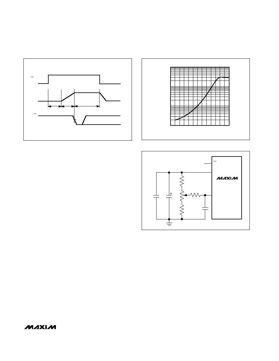
10,000
10
100
1000
fg18c
CONVERSIONS PER SECOND
SUPPLY
CURRENT
(
A)
50
200
1k
5k
20k
100k
Figure 18c. Average Supply Current vs. Conversion Rate,
Powering Down Between Conversions
MAX191
VREF
REFADJ
PD
1
5
6
0.1
F
4.7
F
5k
11k
15k
100k
0.01
F
Figure 19a. External-Compensation Mode with Internal
Reference Adjustment Circuit
相关PDF资料 |
PDF描述 |
|---|---|
| MC10EP89DTR2G | IC DRIVER COAX CBL 5V ECL 8TSSOP |
| V48A36T500BF3 | CONVERTER MOD DC/DC 36V 500W |
| V48A24T500B2 | CONVERTER MOD DC/DC 24V 500W |
| MAX110AEPE+ | IC ADC SERIAL 2CH 14BIT 16-DIP |
| MS3106R20-8S | CONN PLUG 6POS STRAIGHT W/SCKT |
相关代理商/技术参数 |
参数描述 |
|---|---|
| MAX191AENG | 功能描述:模数转换器 - ADC RoHS:否 制造商:Texas Instruments 通道数量:2 结构:Sigma-Delta 转换速率:125 SPs to 8 KSPs 分辨率:24 bit 输入类型:Differential 信噪比:107 dB 接口类型:SPI 工作电源电压:1.7 V to 3.6 V, 2.7 V to 5.25 V 最大工作温度:+ 85 C 安装风格:SMD/SMT 封装 / 箱体:VQFN-32 |
| MAX191AENG+ | 功能描述:模数转换器 - ADC RoHS:否 制造商:Texas Instruments 通道数量:2 结构:Sigma-Delta 转换速率:125 SPs to 8 KSPs 分辨率:24 bit 输入类型:Differential 信噪比:107 dB 接口类型:SPI 工作电源电压:1.7 V to 3.6 V, 2.7 V to 5.25 V 最大工作温度:+ 85 C 安装风格:SMD/SMT 封装 / 箱体:VQFN-32 |
| MAX191AEWG | 功能描述:模数转换器 - ADC RoHS:否 制造商:Texas Instruments 通道数量:2 结构:Sigma-Delta 转换速率:125 SPs to 8 KSPs 分辨率:24 bit 输入类型:Differential 信噪比:107 dB 接口类型:SPI 工作电源电压:1.7 V to 3.6 V, 2.7 V to 5.25 V 最大工作温度:+ 85 C 安装风格:SMD/SMT 封装 / 箱体:VQFN-32 |
| MAX191AEWG+ | 功能描述:模数转换器 - ADC RoHS:否 制造商:Texas Instruments 通道数量:2 结构:Sigma-Delta 转换速率:125 SPs to 8 KSPs 分辨率:24 bit 输入类型:Differential 信噪比:107 dB 接口类型:SPI 工作电源电压:1.7 V to 3.6 V, 2.7 V to 5.25 V 最大工作温度:+ 85 C 安装风格:SMD/SMT 封装 / 箱体:VQFN-32 |
| MAX191AEWG+T | 功能描述:模数转换器 - ADC RoHS:否 制造商:Texas Instruments 通道数量:2 结构:Sigma-Delta 转换速率:125 SPs to 8 KSPs 分辨率:24 bit 输入类型:Differential 信噪比:107 dB 接口类型:SPI 工作电源电压:1.7 V to 3.6 V, 2.7 V to 5.25 V 最大工作温度:+ 85 C 安装风格:SMD/SMT 封装 / 箱体:VQFN-32 |
发布紧急采购,3分钟左右您将得到回复。