- 您现在的位置:买卖IC网 > PDF目录9869 > MAX191ACWG+T (Maxim Integrated Products)IC ADC 12BIT 100KSPS 24-SOIC PDF资料下载
参数资料
| 型号: | MAX191ACWG+T |
| 厂商: | Maxim Integrated Products |
| 文件页数: | 2/24页 |
| 文件大小: | 0K |
| 描述: | IC ADC 12BIT 100KSPS 24-SOIC |
| 产品培训模块: | Lead (SnPb) Finish for COTS Obsolescence Mitigation Program |
| 标准包装: | 1,000 |
| 位数: | 12 |
| 采样率(每秒): | 100k |
| 数据接口: | MICROWIRE?,并联,QSPI?,串行,SPI? |
| 转换器数目: | 1 |
| 功率耗散(最大): | 941mW |
| 电压电源: | 双 ± |
| 工作温度: | 0°C ~ 70°C |
| 安装类型: | 表面贴装 |
| 封装/外壳: | 24-SOIC(0.295",7.50mm 宽) |
| 供应商设备封装: | 24-SOIC W |
| 包装: | 带卷 (TR) |
| 输入数目和类型: | 2 个单端,单极;2 个单端,双极;1 个差分,单极;1 个差分,双极 |
MAX191
between 45% and 55%.
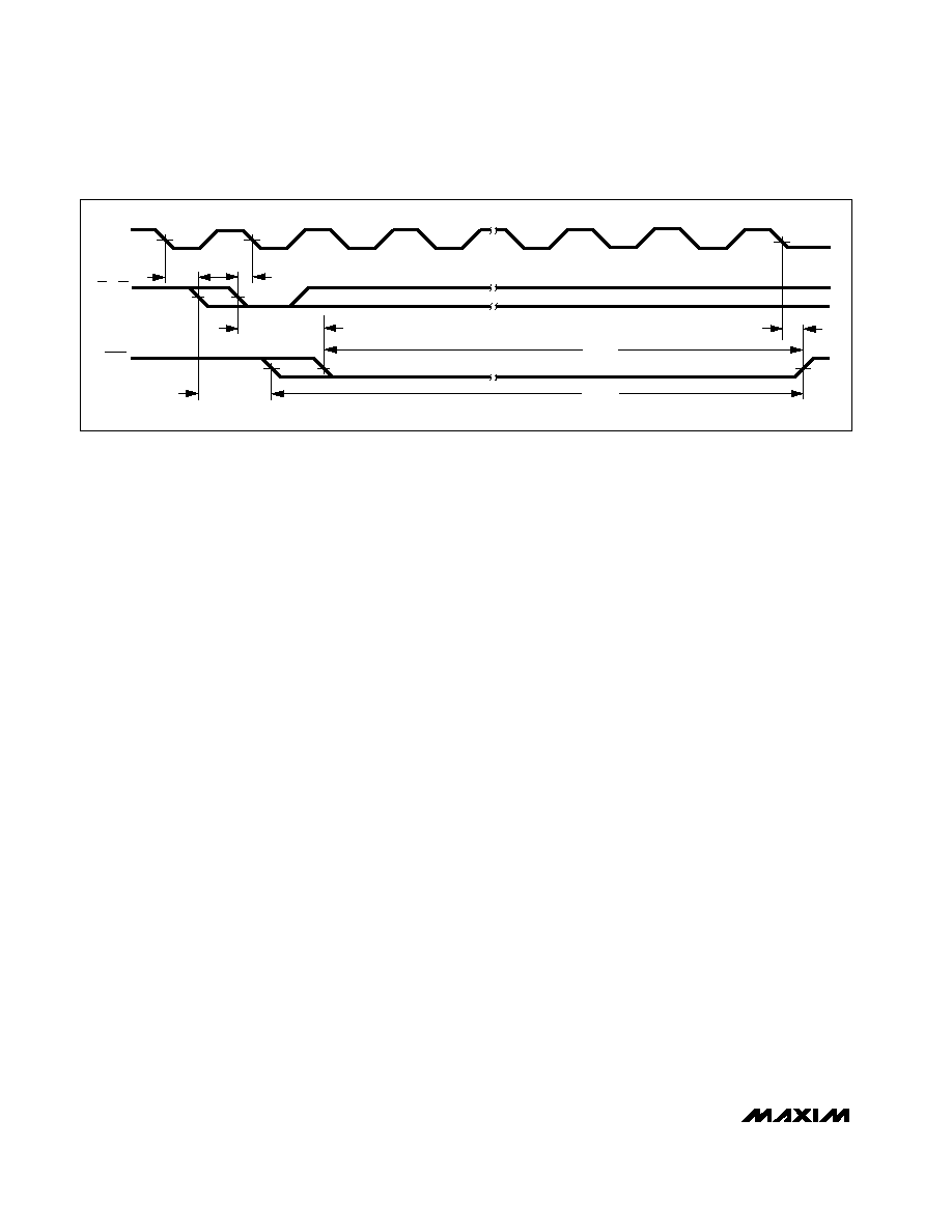
Clock and Control Synchronization
For best analog performance on the MAX191, the clock
should be synchronized to the conversion start signals
(CS and RD) as shown in Figure 6. A conversion should
not be started in the 50ns before a clock edge nor in
the 100ns after it. This ensures that CLK transitions are
not coupled to the analog input and sampled by the
T/H. The magnitude of this feedthrough can be a few
millivolts. When the clock and conversion start signals
are synchronized, small end-point errors (offset and
full-scale) are the most that can be generated by clock
feedthrough. Even these errors (which can be trimmed
out) can be avoided by ensuring that the start of a con-
version (RD or CS falling edge) does not occur close to
a clock transition (Figure 6), as described above.
Parallel Digital-Interface Mode
Output-Data Format
The data output from the MAX191 is straight binary in
the unipolar mode. In the bipolar mode, the MSB is
inverted (see Figure 22). The 12 data bits can be out-
put either in two 8-bit bytes or as a serial output. Table
1 shows the data-bus output format.
A 2-byte read uses outputs D7–D0. Byte selection is
controlled by HBEN. When HBEN is low, the lower 8
bits appear at the data outputs. When HBEN is high,
the upper 4 bits appear at D0-D3 with the leading 4 bits
low in locations D4–D7.
Timing and Control
Conversion-start and data-read operations are con-
trolled by the HBEN, CS, and RD digital inputs. A logic
low is required on all three inputs to start a conversion,
and once the conversion is in progress it cannot be
restarted. BUSY remains low during the entire conver-
sion cycle.
The timing diagrams of Figures 7–10 outline two paral-
lel-interface modes and one serial mode.
Slow-Memory Mode
In slow-memory mode, the device appears to the P as
a slow peripheral or memory. Conversion is initiated
with a read instruction (see Figure 7 and Table 2). Set
the PAR pin high for parallel interface mode. Beginning
with HBEN low, taking CS and RD low starts the con-
version. The analog input is sampled on the falling
edge of RD. BUSY remains low while the conversion is
in progress. The previous conversion result appears at
the digital outputs until the end of conversion, when
BUSY returns high. The output latches are then updat-
ed with the newest results of the 8 LSBs on D7–D0. A
second read operation with HBEN high places the 4
MSBs, with 4 leading 0s, on data outputs D7–D0. The
second read operation does not start a new conversion
because HBEN is high.
ROM Mode
As in slow-memory mode, D7–D0 are used for 2-byte
reads. A conversion starts with a read instruction with
HBEN and CS low. The T/H samples the input on the
falling edge of RD (see Figure 8 and Table 3). PAR is set
high. At this point the data outputs contain the 8 LSBs
from the previous conversion. Two more read operations
are needed to access the conversion result. The first
occurs with HBEN high, where the 4 MSBs with 4 leading
0s are accessed. The second read, with HBEN low, out-
puts the 8 LSBs and also starts a new conversion.
Figure 9 and Table 4 show how to read output data
within one conversion cycle without starting another
conversion. Trigger the falling edge of a read on the ris-
Low-Power, 12-Bit Sampling ADC
with Internal Reference and Power-Down
10
______________________________________________________________________________________
tCONV
CS + RD
BUSY
t16
CLK
t17
t2
t13
t2
tCONV
Figure 6. CS, RD, and CLK Synchronous Operation
相关PDF资料 |
PDF描述 |
|---|---|
| MC10EP89DTR2G | IC DRIVER COAX CBL 5V ECL 8TSSOP |
| V48A36T500BF3 | CONVERTER MOD DC/DC 36V 500W |
| V48A24T500B2 | CONVERTER MOD DC/DC 24V 500W |
| MAX110AEPE+ | IC ADC SERIAL 2CH 14BIT 16-DIP |
| MS3106R20-8S | CONN PLUG 6POS STRAIGHT W/SCKT |
相关代理商/技术参数 |
参数描述 |
|---|---|
| MAX191AENG | 功能描述:模数转换器 - ADC RoHS:否 制造商:Texas Instruments 通道数量:2 结构:Sigma-Delta 转换速率:125 SPs to 8 KSPs 分辨率:24 bit 输入类型:Differential 信噪比:107 dB 接口类型:SPI 工作电源电压:1.7 V to 3.6 V, 2.7 V to 5.25 V 最大工作温度:+ 85 C 安装风格:SMD/SMT 封装 / 箱体:VQFN-32 |
| MAX191AENG+ | 功能描述:模数转换器 - ADC RoHS:否 制造商:Texas Instruments 通道数量:2 结构:Sigma-Delta 转换速率:125 SPs to 8 KSPs 分辨率:24 bit 输入类型:Differential 信噪比:107 dB 接口类型:SPI 工作电源电压:1.7 V to 3.6 V, 2.7 V to 5.25 V 最大工作温度:+ 85 C 安装风格:SMD/SMT 封装 / 箱体:VQFN-32 |
| MAX191AEWG | 功能描述:模数转换器 - ADC RoHS:否 制造商:Texas Instruments 通道数量:2 结构:Sigma-Delta 转换速率:125 SPs to 8 KSPs 分辨率:24 bit 输入类型:Differential 信噪比:107 dB 接口类型:SPI 工作电源电压:1.7 V to 3.6 V, 2.7 V to 5.25 V 最大工作温度:+ 85 C 安装风格:SMD/SMT 封装 / 箱体:VQFN-32 |
| MAX191AEWG+ | 功能描述:模数转换器 - ADC RoHS:否 制造商:Texas Instruments 通道数量:2 结构:Sigma-Delta 转换速率:125 SPs to 8 KSPs 分辨率:24 bit 输入类型:Differential 信噪比:107 dB 接口类型:SPI 工作电源电压:1.7 V to 3.6 V, 2.7 V to 5.25 V 最大工作温度:+ 85 C 安装风格:SMD/SMT 封装 / 箱体:VQFN-32 |
| MAX191AEWG+T | 功能描述:模数转换器 - ADC RoHS:否 制造商:Texas Instruments 通道数量:2 结构:Sigma-Delta 转换速率:125 SPs to 8 KSPs 分辨率:24 bit 输入类型:Differential 信噪比:107 dB 接口类型:SPI 工作电源电压:1.7 V to 3.6 V, 2.7 V to 5.25 V 最大工作温度:+ 85 C 安装风格:SMD/SMT 封装 / 箱体:VQFN-32 |
发布紧急采购,3分钟左右您将得到回复。