- 您现在的位置:买卖IC网 > PDF目录383342 > MAX194AMDE (MAXIM INTEGRATED PRODUCTS INC) 14-Bit, 85ksps ADC with 10A Shutdown PDF资料下载
参数资料
| 型号: | MAX194AMDE |
| 厂商: | MAXIM INTEGRATED PRODUCTS INC |
| 元件分类: | ADC |
| 英文描述: | 14-Bit, 85ksps ADC with 10A Shutdown |
| 中文描述: | 1-CH 14-BIT SUCCESSIVE APPROXIMATION ADC, SERIAL ACCESS, CDIP16 |
| 封装: | SIDEBRAZED, CERAMIC, DIP-16 |
| 文件页数: | 15/24页 |
| 文件大小: | 223K |
| 代理商: | MAX194AMDE |
Input Acquisition and Settling
Four conversion-clock periods are allocated for acquir-
ing the input signal. At the highest conversion rate, four
clock periods is 2.4μs. If more than three clock cycles
have occurred since the end of the previous conver-
sion, conversion begins on the next falling clock edge
after
CONV
goes low. Otherwise, bringing
CONV
low
begins a conversion on the fourth falling clock edge
after the previous conversion. This scheme ensures the
minimum input acquisition time is four clock periods.
Most applications require an input buffer amplifier. If
the input signal is multiplexed, the input channel should
be switched near the beginning of a conversion, rather
than near the end of or after a conversion (Figure 13).
This allows time for the input buffer amplifier to respond
to a large step change in input signal. The input amplifi-
er must have a high enough slew rate to complete the
required output voltage change before the beginning of
the acquisition time.
At the beginning of acquisition, the capacitive DAC is
connected to the amplifier output, causing some output
disturbance. Ensure that the sampled voltage has set-
tled to within the required limits before the end of the
acquisition time. If the frequency of interest is low, AIN
can be bypassed with a large enough capacitor to
charge the capacitive DAC with very little change in
voltage (Figure 14). However, for AC use, AIN must be
driven by a wideband buffer (at least 10MHz), which
must be stable with the DAC’s capacitive load (in paral-
lel with any AIN bypass capacitor used) and also must
settle quickly (Figure 15 or 16).
Digital Noise
Digital noise can easily be coupled to AIN and REF.
The conversion clock (CLK) and other digital signals
that are active during input acquisition contribute noise
to the conversion result. If the noise signal is synchro-
nous to the sampling interval, an effective input offset is
produced. Asynchronous signals produce random
noise on the input, whose high-frequency components
may be aliased into the frequency band of interest.
Minimize noise by presenting a low impedance (at the
frequencies contained in the noise signal) at the inputs.
This requires bypassing AIN to AGND, or buffering the
input with an amplifier that has a small-signal band-
width of several megahertz, or preferably both. AIN has
a bandwidth of about 16MHz.
Offsets resulting from synchronous noise (such as the
conversion clock) are canceled by the MAX194’s cali-
bration scheme. However, because the magnitude of
the offset produced by a synchronous signal depends
on the signal’s shape, recalibration may be appropriate
if the shape or relative timing of the clock or other digi-
tal signals change, as might occur if more than one
clock signal or frequency is used.
Distortion
Avoid degrading dynamic performance by choosing an
amplifier with distortion much less than the MAX194’s
THD (-90dB, or 0.0032%) at frequencies of interest. If
the chosen amplifier has insufficient common-mode
rejection, which results in degraded THD performance,
use the inverting configuration (positive input ground-
ed) to eliminate errors from this source. Low tempera-
ture-coefficient, gain-setting resistors reduce linearity
errors caused by resistance changes due to self-heat-
ing. Also, to reduce linearity errors due to finite amplifier
gain, use an amplifier circuit with sufficient loop gain at
the frequencies of interest (Figures 14, 15, 16).
M
14-Bit, 85ksps ADC with 10μA S hutdown
______________________________________________________________________________________
15
MAX410
4
7
6
2
3
IN
+5V
-5V
0.1
μ
F
0.01
μ
F
22
510
0.1
μ
F
AIN
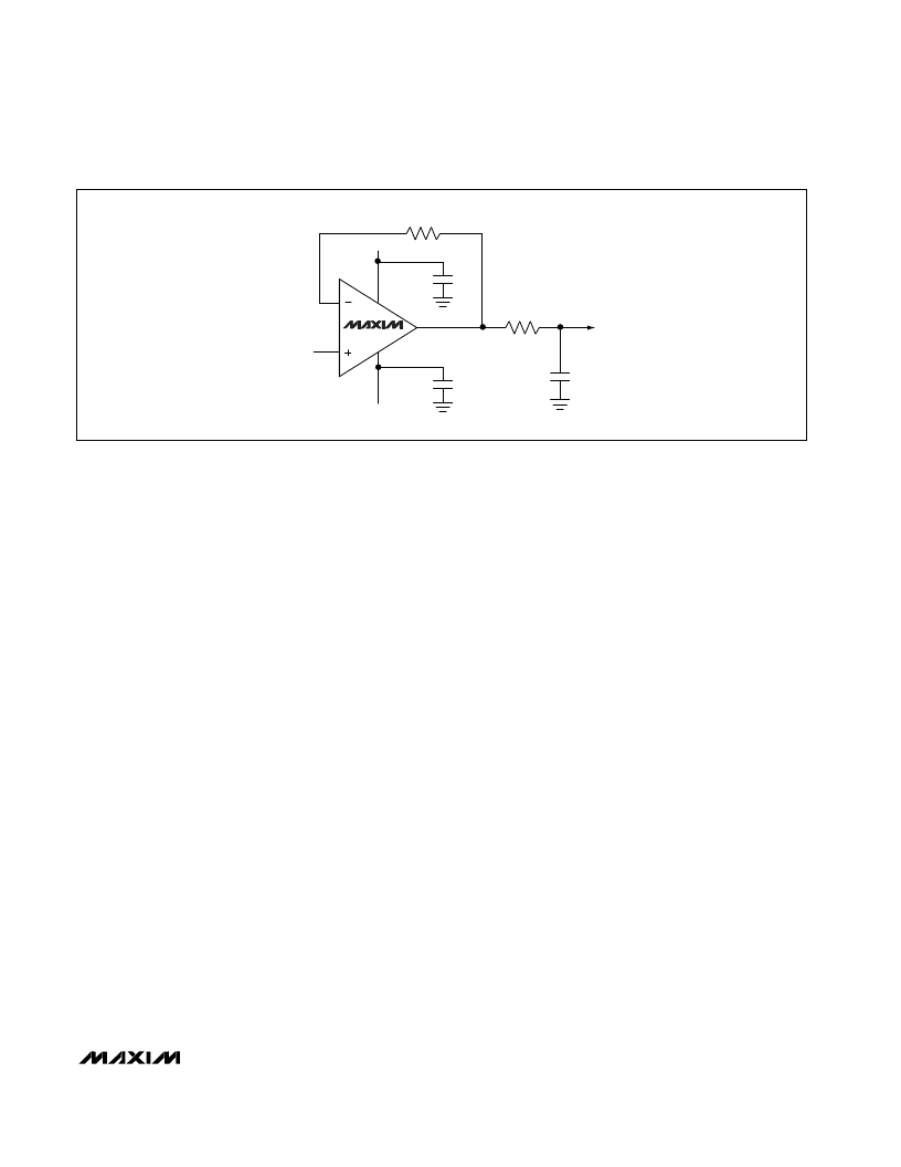
Figure 16. ±5V Buffer for AC/DC Use Has ±3.5V Swing
相关PDF资料 |
PDF描述 |
|---|---|
| MAX194BEPE | Fixed-Point Digital Signal Processor 532-FCBGA |
| MAX194BEWE | 14-Bit, 85ksps ADC with 10A Shutdown |
| MAX194BMDE | 14-Bit, 85ksps ADC with 10A Shutdown |
| MAX195ACDE | 16-Bit, 85ksps ADC with 10レA Shutdown |
| MAX195AEDE | 16-Bit, 85ksps ADC with 10レA Shutdown |
相关代理商/技术参数 |
参数描述 |
|---|---|
| MAX194BCPE | 功能描述:模数转换器 - ADC RoHS:否 制造商:Texas Instruments 通道数量:2 结构:Sigma-Delta 转换速率:125 SPs to 8 KSPs 分辨率:24 bit 输入类型:Differential 信噪比:107 dB 接口类型:SPI 工作电源电压:1.7 V to 3.6 V, 2.7 V to 5.25 V 最大工作温度:+ 85 C 安装风格:SMD/SMT 封装 / 箱体:VQFN-32 |
| MAX194BCPE+ | 功能描述:模数转换器 - ADC 14Bit 85ksps 5V Precision ADC RoHS:否 制造商:Texas Instruments 通道数量:2 结构:Sigma-Delta 转换速率:125 SPs to 8 KSPs 分辨率:24 bit 输入类型:Differential 信噪比:107 dB 接口类型:SPI 工作电源电压:1.7 V to 3.6 V, 2.7 V to 5.25 V 最大工作温度:+ 85 C 安装风格:SMD/SMT 封装 / 箱体:VQFN-32 |
| MAX194BCWE | 功能描述:模数转换器 - ADC Integrated Circuits (ICs) RoHS:否 制造商:Texas Instruments 通道数量:2 结构:Sigma-Delta 转换速率:125 SPs to 8 KSPs 分辨率:24 bit 输入类型:Differential 信噪比:107 dB 接口类型:SPI 工作电源电压:1.7 V to 3.6 V, 2.7 V to 5.25 V 最大工作温度:+ 85 C 安装风格:SMD/SMT 封装 / 箱体:VQFN-32 |
| MAX194BCWE+ | 功能描述:模数转换器 - ADC 14Bit 85ksps 5V Precision ADC RoHS:否 制造商:Texas Instruments 通道数量:2 结构:Sigma-Delta 转换速率:125 SPs to 8 KSPs 分辨率:24 bit 输入类型:Differential 信噪比:107 dB 接口类型:SPI 工作电源电压:1.7 V to 3.6 V, 2.7 V to 5.25 V 最大工作温度:+ 85 C 安装风格:SMD/SMT 封装 / 箱体:VQFN-32 |
| MAX194BCWE+T | 功能描述:模数转换器 - ADC 14Bit 85ksps 5V Precision ADC RoHS:否 制造商:Texas Instruments 通道数量:2 结构:Sigma-Delta 转换速率:125 SPs to 8 KSPs 分辨率:24 bit 输入类型:Differential 信噪比:107 dB 接口类型:SPI 工作电源电压:1.7 V to 3.6 V, 2.7 V to 5.25 V 最大工作温度:+ 85 C 安装风格:SMD/SMT 封装 / 箱体:VQFN-32 |
发布紧急采购,3分钟左右您将得到回复。