- 您现在的位置:买卖IC网 > PDF目录10495 > MAX19515ETM+ (Maxim Integrated Products)IC ADC 10BIT 65MSPS DUAL 48TQFN PDF资料下载
参数资料
| 型号: | MAX19515ETM+ |
| 厂商: | Maxim Integrated Products |
| 文件页数: | 17/35页 |
| 文件大小: | 0K |
| 描述: | IC ADC 10BIT 65MSPS DUAL 48TQFN |
| 产品培训模块: | Lead (SnPb) Finish for COTS Obsolescence Mitigation Program |
| 标准包装: | 43 |
| 位数: | 10 |
| 采样率(每秒): | 65M |
| 数据接口: | 串行,并联 |
| 转换器数目: | 2 |
| 电压电源: | 模拟和数字 |
| 工作温度: | -40°C ~ 85°C |
| 安装类型: | 表面贴装 |
| 封装/外壳: | 48-WFQFN 裸露焊盘 |
| 供应商设备封装: | 48-TQFN-EP(7x7) |
| 包装: | 托盘 |
| 输入数目和类型: | 4 个单端,单极;2 个差分,单极 |
| 产品目录页面: | 1398 (CN2011-ZH PDF) |
第1页第2页第3页第4页第5页第6页第7页第8页第9页第10页第11页第12页第13页第14页第15页第16页当前第17页第18页第19页第20页第21页第22页第23页第24页第25页第26页第27页第28页第29页第30页第31页第32页第33页第34页第35页
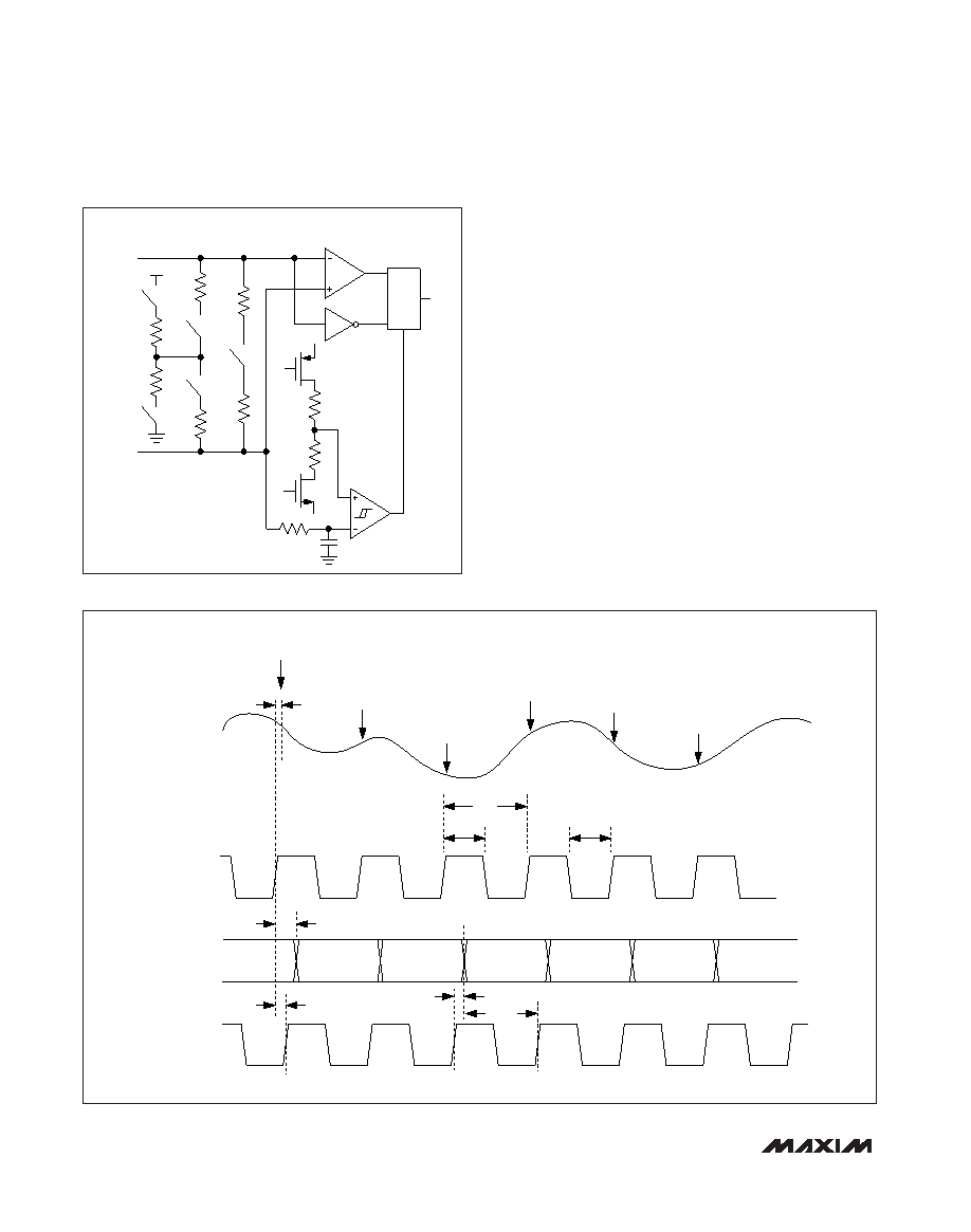
Clock Inputs
The input clock interface provides for flexibility in the
requirements of the clock driver. The MAX19515
accepts a fully differential clock or single-ended logic-
level clock. For differential clock operation, connect a
differential clock to the CLK+ and CLK- inputs. In this
mode, the input common mode is established internally
to allow for AC-coupling. The differential clock signal
can also be DC-coupled if the common mode is con-
strained to the specified 1V to 1.4V clock input com-
mon-mode range. For single-ended operation, connect
CLK- to GND and drive the CLK+ input with a logic-
level signal. When the CLK- input is grounded (or
pulled below the threshold of the clock mode detection
comparator) the differential-to-single-ended conversion
stage is disabled and the logic-level inverter path is
activated.
Clock Divider
The MAX19515 offers a clock-divider option. Enable
clock division either by setting DIV0 and DIV1 through
the serial interface; see the Clock Divide/Data
MAX19515
Dual-Channel, 10-Bit, 65Msps ADC
24
______________________________________________________________________________________
CLK+
100
TERMINATION
(PROGRAMMABLE)
SELF-BIAS TURNED OFF FOR
SINGLE-ENDED CLOCK
OR POWER-DOWN.
CLK-
GND
AVDD
10k
20k
5k
5k
50
50
2:1 MUX
SELECT
THRESHOLD
Figure 8. Simplified Clock Input Schematic
DCLK
DATA, DOR
SAMPLE CLOCK
n
n+1
SAMPLE ON RISING EDGE
n+2
n+4
n+5
n-9
n-8
n-10
n-7
n-6
n-5
n-4
tCLK
tSETUP
tCH
tDD
tDC
tHOLD
tCL
DUAL-BUS OUTPUT MODE
SAMPLE CLOCK IS THE DERIVED CLOCK FROM (CLK+ - CLK-)/CLOCK DIVIDER, IN_ = IN_+ - IN_-.
SAMPLING
INSTANT
SAMPLING
INSTANT
SAMPLING
INSTANT
SAMPLING
INSTANT
SAMPLING
INSTANT
SAMPLING
INSTANT
IN_
tAD
n+3
Figure 9. Dual-Bus Output Mode Timing
相关PDF资料 |
PDF描述 |
|---|---|
| VI-BT1-IV-F3 | CONVERTER MOD DC/DC 12V 150W |
| MX7576KP+ | IC ADC 8BIT MPU COMP 20-PLCC |
| VI-BT1-IV-F2 | CONVERTER MOD DC/DC 12V 150W |
| VI-BT1-IV-F1 | CONVERTER MOD DC/DC 12V 150W |
| MX7574KN+ | IC ADC 8BIT MPU COMP 18-DIP |
相关代理商/技术参数 |
参数描述 |
|---|---|
| MAX19515ETM/V+ | 功能描述:模数转换器 - ADC Dual-Channel 10-Bit 65Msps ADC RoHS:否 制造商:Texas Instruments 通道数量:2 结构:Sigma-Delta 转换速率:125 SPs to 8 KSPs 分辨率:24 bit 输入类型:Differential 信噪比:107 dB 接口类型:SPI 工作电源电压:1.7 V to 3.6 V, 2.7 V to 5.25 V 最大工作温度:+ 85 C 安装风格:SMD/SMT 封装 / 箱体:VQFN-32 |
| MAX19515ETM/V+T | 功能描述:模数转换器 - ADC Dual-Channel 10-Bit 65Msps ADC RoHS:否 制造商:Texas Instruments 通道数量:2 结构:Sigma-Delta 转换速率:125 SPs to 8 KSPs 分辨率:24 bit 输入类型:Differential 信噪比:107 dB 接口类型:SPI 工作电源电压:1.7 V to 3.6 V, 2.7 V to 5.25 V 最大工作温度:+ 85 C 安装风格:SMD/SMT 封装 / 箱体:VQFN-32 |
| MAX19515ETM+ | 功能描述:模数转换器 - ADC 10-Bit 2Ch 65Msps 1.8V Precision ADC RoHS:否 制造商:Texas Instruments 通道数量:2 结构:Sigma-Delta 转换速率:125 SPs to 8 KSPs 分辨率:24 bit 输入类型:Differential 信噪比:107 dB 接口类型:SPI 工作电源电压:1.7 V to 3.6 V, 2.7 V to 5.25 V 最大工作温度:+ 85 C 安装风格:SMD/SMT 封装 / 箱体:VQFN-32 |
| MAX19515ETM+T | 功能描述:模数转换器 - ADC 10-Bit 2Ch 65Msps 1.8V Precision ADC RoHS:否 制造商:Texas Instruments 通道数量:2 结构:Sigma-Delta 转换速率:125 SPs to 8 KSPs 分辨率:24 bit 输入类型:Differential 信噪比:107 dB 接口类型:SPI 工作电源电压:1.7 V to 3.6 V, 2.7 V to 5.25 V 最大工作温度:+ 85 C 安装风格:SMD/SMT 封装 / 箱体:VQFN-32 |
| MAX19515EVKIT+ | 功能描述:数据转换 IC 开发工具 MAX19505-07/15-17 Eval Kit RoHS:否 制造商:Texas Instruments 产品:Demonstration Kits 类型:ADC 工具用于评估:ADS130E08 接口类型:SPI 工作电源电压:- 6 V to + 6 V |
发布紧急采购,3分钟左右您将得到回复。