- 您现在的位置:买卖IC网 > PDF目录14545 > MAX1951ESA+T (Maxim Integrated Products)IC REG BUCK SYNC ADJ 2A 8SOIC PDF资料下载
参数资料
| 型号: | MAX1951ESA+T |
| 厂商: | Maxim Integrated Products |
| 文件页数: | 7/15页 |
| 文件大小: | 0K |
| 描述: | IC REG BUCK SYNC ADJ 2A 8SOIC |
| 产品培训模块: | Lead (SnPb) Finish for COTS Obsolescence Mitigation Program |
| 标准包装: | 2,500 |
| 类型: | 降压(降压) |
| 输出类型: | 可调式 |
| 输出数: | 1 |
| 输出电压: | 0.8 V ~ 5.5 V |
| 输入电压: | 2.6 V ~ 5.5 V |
| PWM 型: | 电流模式 |
| 频率 - 开关: | 1MHz |
| 电流 - 输出: | 2A |
| 同步整流器: | 是 |
| 工作温度: | -40°C ~ 85°C |
| 安装类型: | 表面贴装 |
| 封装/外壳: | 8-SOIC(0.154",3.90mm 宽) |
| 包装: | 带卷 (TR) |
| 供应商设备封装: | 8-SOIC |
�� �
�
�1MHz,� All-Ceramic,� 2.6V� to� 5.5V� Input,�
�2A� PWM� Step-Down� DC-to-DC� Regulators�
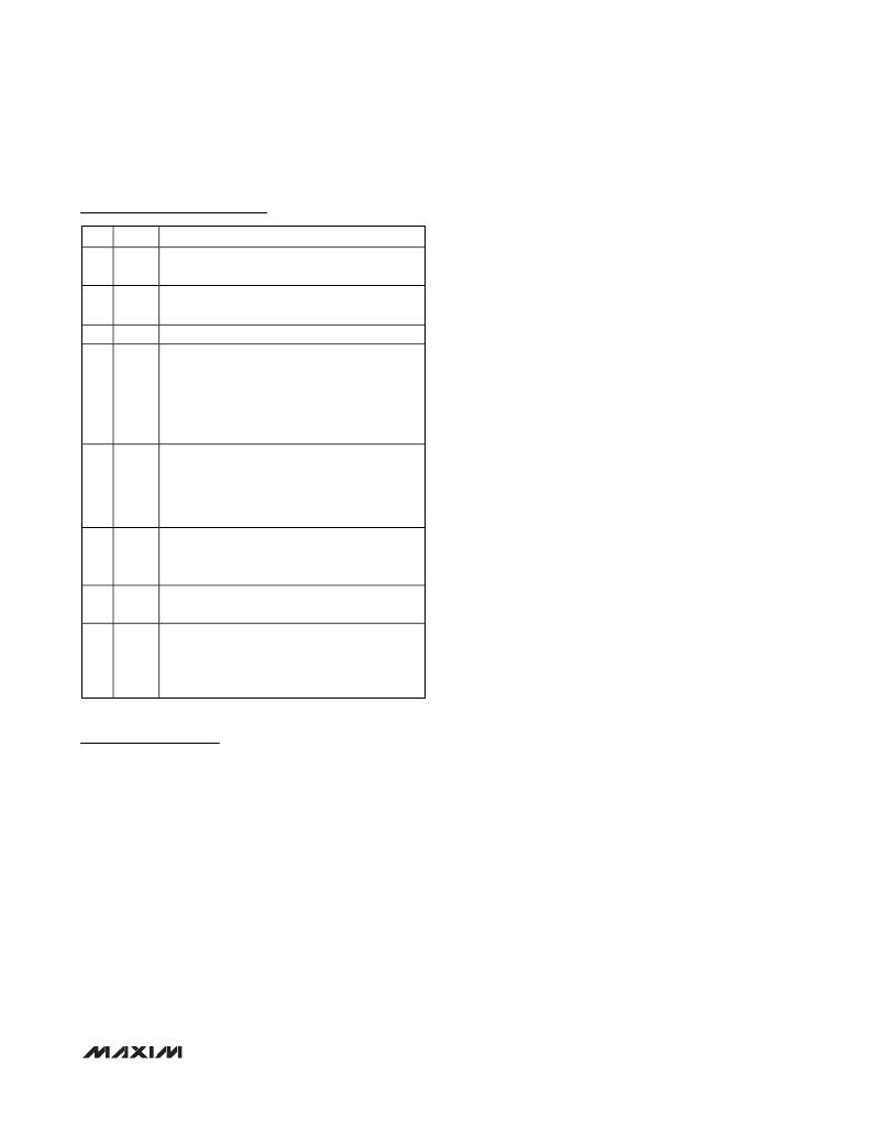
�Pin� Description�
�Controller� Block� Function�
�The� MAX1951/MAX1952� step-down� converters� use� a�
�PIN� NAME�
�FUNCTION�
�PWM� current-mode� control� scheme.� An� open-loop� com-�
�1�
�2�
�3�
�4�
�V� CC�
�REF�
�GND�
�FB�
�Supply� Voltage.� Bypass� V� CC� with� 0.1μF�
�capacitor� to� ground� and� 10� Ω� resistor� to� IN.�
�Reference� Bypass.� Bypass� REF� with� 0.1μF�
�capacitor� to� ground.�
�Ground�
�Feedback� Input.� Connect� FB� to� the� output� to�
�regulate� using� the� internal� feedback� resistor�
�string� (MAX1952).� Connect� an� external� resistor-�
�divider� from� the� output� to� FB� and� GND� to� set�
�the� output� to� a� voltage� between� 0.8V� and� V� IN�
�(MAX1951).�
�Regulator� Compensation.� Connect� series� RC�
�network� from� COMP� to� GND.� Pull� COMP� below�
�parator� compares� the� integrated� voltage-feedback� signal�
�against� the� sum� of� the� amplified� current-sense� signal� and�
�the� slope� compensation� ramp.� At� each� rising� edge� of� the�
�internal� clock,� the� internal� high-side� MOSFET� turns� on�
�until� the� PWM� comparator� trips.� During� this� on-time,� cur-�
�rent� ramps� up� through� the� inductor,� sourcing� current� to�
�the� output� and� storing� energy� in� the� inductor.� The� current-�
�mode� feedback� system� regulates� the� peak� inductor� cur-�
�rent� as� a� function� of� the� output� voltage� error� signal.� Since�
�the� average� inductor� current� is� nearly� the� same� as� the�
�peak� inductor� current� (<30%� ripple� current),� the� circuit�
�acts� as� a� switch-mode� transconductance� amplifier.� To�
�preserve� inner-loop� stability� and� eliminate� inductor� stair-�
�casing,� a� slope-compensation� ramp� is� summed� into� the�
�main� PWM� comparator.� During� the� second� half� of� the�
�5�
�6�
�COMP� 0.17V� to� shut� down� the� regulator.� COMP� =�
�GND� when� V� IN� is� less� than� 2.25V� (see� the�
�Compensation� and� Shutdown� Mode� section)�
�Power� Ground.� Internally� connected� to� GND.�
�PGND� Keep� power� ground� and� signal� ground� planes�
�separate.�
�cycle,� the� internal� high-side� p-channel� MOSFET� turns� off,�
�and� the� internal� low-side� n-channel� MOSFET� turns� on.�
�The� inductor� releases� the� stored� energy� as� its� current�
�ramps� down� while� still� providing� current� to� the� output.� The�
�output� capacitor� stores� charge� when� the� inductor� current�
�exceeds� the� load� current,� and� discharges� when� the�
�inductor� current� is� lower,� smoothing� the� voltage� across�
�7�
�8�
�LX�
�IN�
�Inductor� Connection.� Connect� an� inductor�
�between� LX� and� the� regulator� output.�
�Power-Supply� Voltage.� Input� voltage� range�
�from� 2.6V� to� 5.5V.� Bypass� IN� with� a� 10μF� (min)�
�ceramic� capacitor� to� GND� and� a� 10� Ω� resistor�
�to� V� CC� .�
�the� load.� Under� overload� conditions,� when� the� inductor�
�current� exceeds� the� current� limit� (see� the� Current� Limit�
�section),� the� high-side� MOSFET� does� not� turn� on� at� the�
�rising� edge� of� the� clock� and� the� low-side� MOSFET�
�remains� on� to� let� the� inductor� current� ramp� down.�
�Current� Sense�
�An� internal� current-sense� amplifier� produces� a� current�
�signal� proportional� to� the� voltage� generated� by� the�
�Detailed� Description�
�The� MAX1951/MAX1952� high-efficiency� switching� regula-�
�tors� are� small,� simple,� DC-to-DC� step-down� converters�
�capable� of� delivering� up� to� 2A� of� output� current.� The�
�devices� operate� in� pulse-width� modulation� (PWM)� at� a�
�fixed� frequency� of� 1MHz� from� a� 2.6V� to� 5.5V� input� voltage�
�and� provide� an� output� voltage� from� 0.8V� to� V� IN� ,� making�
�the� MAX1951/MAX1952� ideal� for� on-board� postregula-�
�tion� applications.� The� high� switching� frequency� allows�
�for� the� use� of� smaller� external� components,� and� internal�
�synchronous� rectifiers� improve� efficiency� and� eliminate�
�the� typical� Schottky� free-wheeling� diode.� Using� the� on-�
�resistance� of� the� internal� high-side� MOSFET� to� sense�
�switching� currents� eliminates� current-sense� resistors,�
�further� improving� efficiency� and� cost.� The� MAX1951�
�total� output� error� over� load,� line,� and� temperature� (0°C�
�to� +85°C)� is� less� than� 1%.�
�high-side� MOSFET� on-resistance� and� the� inductor� cur-�
�rent� (R� DS(ON)� x� I� LX� ).� The� amplified� current-sense� signal�
�and� the� internal� slope� compensation� signal� are�
�summed� together� into� the� comparator’s� inverting� input.�
�The� PWM� comparator� turns� off� the� internal� high-side�
�MOSFET� when� this� sum� exceeds� the� output� from� the�
�voltage-error� amplifier.�
�Current� Limit�
�The� internal� high-side� MOSFET� has� a� current� limit� of� 3.1A�
�(typ).� If� the� current� flowing� out� of� LX� exceeds� this� limit,�
�the� high-side� MOSFET� turns� off� and� the� synchronous�
�rectifier� turns� on.� This� lowers� the� duty� cycle� and� causes�
�the� output� voltage� to� droop� until� the� current� limit� is� no�
�longer� exceeded.� A� synchronous� rectifier� current� limit� of�
�-0.6A� (typ)� protects� the� device� from� current� flowing� into�
�LX.� If� the� negative� current� limit� is� exceeded,� the� synchro-�
�nous� rectifier� turns� off,� forcing� the� inductor� current� to� flow�
�_______________________________________________________________________________________�
�7�
�相关PDF资料 |
PDF描述 |
|---|---|
| GMC20DRTN | CONN EDGECARD 40POS DIP .100 SLD |
| GSC20DRTH | CONN EDGECARD 40POS DIP .100 SLD |
| GMC20DRTH | CONN EDGECARD 40POS DIP .100 SLD |
| GCC31DRTF | CONN EDGECARD 62POS DIP .100 SLD |
| EMC15DRYS | CONN EDGECARD 30POS DIP .100 SLD |
相关代理商/技术参数 |
参数描述 |
|---|---|
| MAX1951ESA-TG05 | 功能描述:直流/直流开关调节器 RoHS:否 制造商:International Rectifier 最大输入电压:21 V 开关频率:1.5 MHz 输出电压:0.5 V to 0.86 V 输出电流:4 A 输出端数量: 最大工作温度: 安装风格:SMD/SMT 封装 / 箱体:PQFN 4 x 5 |
| MAX1951EVKIT | 功能描述:直流/直流开关调节器 Evaluation Kit for the MAX1951 MAX1952 RoHS:否 制造商:International Rectifier 最大输入电压:21 V 开关频率:1.5 MHz 输出电压:0.5 V to 0.86 V 输出电流:4 A 输出端数量: 最大工作温度: 安装风格:SMD/SMT 封装 / 箱体:PQFN 4 x 5 |
| MAX19526EVKIT+ | 制造商:Maxim Integrated Products 功能描述:ANALOG TO DIGITAL CONVERTER - Boxed Product (Development Kits) |
| MAX19526EXE+ | 功能描述:模数转换器 - ADC Integrated Circuits (ICs) Analog to Digital Converters - IC ADC 12BIT 8CH 40MSPS 144CTBGA RoHS:否 制造商:Texas Instruments 通道数量:2 结构:Sigma-Delta 转换速率:125 SPs to 8 KSPs 分辨率:24 bit 输入类型:Differential 信噪比:107 dB 接口类型:SPI 工作电源电压:1.7 V to 3.6 V, 2.7 V to 5.25 V 最大工作温度:+ 85 C 安装风格:SMD/SMT 封装 / 箱体:VQFN-32 |
| MAX19526EXE+T | 功能描述:模数转换器 - ADC Integrated Circuits (ICs) Analog to Digital Converters - IC ADC 12BIT 8CH 40MSPS 144CTBGA RoHS:否 制造商:Texas Instruments 通道数量:2 结构:Sigma-Delta 转换速率:125 SPs to 8 KSPs 分辨率:24 bit 输入类型:Differential 信噪比:107 dB 接口类型:SPI 工作电源电压:1.7 V to 3.6 V, 2.7 V to 5.25 V 最大工作温度:+ 85 C 安装风格:SMD/SMT 封装 / 箱体:VQFN-32 |
发布紧急采购,3分钟左右您将得到回复。