- 您现在的位置:买卖IC网 > PDF目录15488 > MAX1960EEP+ (Maxim Integrated Products)IC REG CTRLR BUCK PWM VM 20-QSOP PDF资料下载
参数资料
| 型号: | MAX1960EEP+ |
| 厂商: | Maxim Integrated Products |
| 文件页数: | 10/29页 |
| 文件大小: | 0K |
| 描述: | IC REG CTRLR BUCK PWM VM 20-QSOP |
| 产品培训模块: | Lead (SnPb) Finish for COTS Obsolescence Mitigation Program |
| 标准包装: | 50 |
| PWM 型: | 电压模式 |
| 输出数: | 1 |
| 频率 - 最大: | 1.12MHz |
| 占空比: | 90% |
| 电源电压: | 2.35 V ~ 5.5 V |
| 降压: | 是 |
| 升压: | 无 |
| 回扫: | 无 |
| 反相: | 无 |
| 倍增器: | 无 |
| 除法器: | 无 |
| Cuk: | 无 |
| 隔离: | 无 |
| 工作温度: | -40°C ~ 85°C |
| 封装/外壳: | 20-SSOP(0.154",3.90mm 宽) |
| 包装: | 管件 |
第1页第2页第3页第4页第5页第6页第7页第8页第9页当前第10页第11页第12页第13页第14页第15页第16页第17页第18页第19页第20页第21页第22页第23页第24页第25页第26页第27页第28页第29页
�� �
�
�2.35V� to� 5.5V,� 0.5%� Accurate,� 1MHz� PWM�
�Step-Down� Controllers� with� Voltage� Margining�
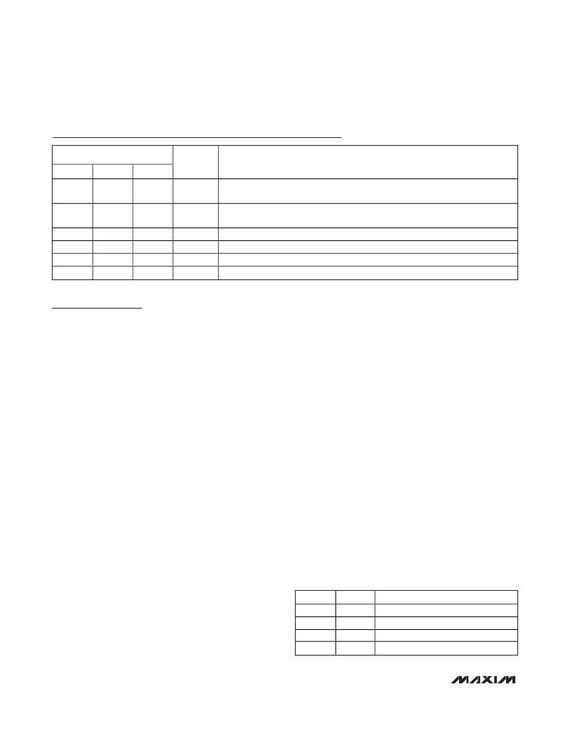
�Pin� Description� (continued)�
�PIN�
�MAX1960� MAX1961� MAX1962�
�NAME�
�FUNCTION�
�15�
�16�
�17�
�18�
�19�
�20�
�15�
�16�
�17�
�18�
�19�
�20�
�15�
�16�
�17�
�18�
�19�
�20�
�C-�
�C+�
�V� CC�
�BST�
�DH�
�LX�
�Charge-Pump� Flying� Capacitor� Negative� Connection.� Use� a� 0.47μF� ceramic�
�capacitor� at� 1MHz,� and� 1μF� between� 450kHz� and� 950kHz.�
�Charge-Pump� Flying� Capacitor� Positive� Connection.� Use� a� 0.47μF� ceramic�
�capacitor� at� 1MHz� and� 1μF� between� 450kHz� and� 950kHz.�
�Input� Supply� to� Charge� Pump�
�Boost� Capacitor� Connection.� Connect� a� 0.1μF� ceramic� capacitor� from� BST� to� LX.�
�High-Side� MOSFET� Gate-Driver� Output.� DH� is� low� in� shutdown.�
�Inductor� Connection�
�Detailed� Description�
�The� MAX1960/MAX1961/MAX1962� are� high-current,�
�high-efficiency� voltage-mode� step-down� DC-DC� con-�
�trollers� that� operate� from� 2.35V� to� 5.5V� input� and� gener-�
�ate� adjustable� voltages� down� to� 0.8V� at� up� to� 20A.� An�
�on-chip� charge� pump� generates� a� regulated� 5V� for� dri-�
�ving� a� variety� of� external� N-channel� MOSFETs.�
�Constant� frequency� PWM� operation� and� external� syn-�
�chronization� make� these� controllers� suitable� for� telecom�
�and� datacom� applications.� The� operating� frequency� is�
�programmed� externally� to� either� 500kHz� or� 1MHz,� or�
�from� 450kHz� to� 1.2MHz� with� an� external� clock.� A� clock�
�output� is� provided� to� synchronize� another� converter� for�
�180°� out-of-phase� operation.�
�A� high� closed-loop� bandwidth� provides� excellent� tran-�
�sient� response� for� applications� with� dynamic� loads.�
�Internal� Charge� Pump�
�An� on-chip� regulated� charge� pump� develops� 5V� at�
�50mA� (max)� with� input� voltages� as� low� as� 2.35V.� The�
�output� of� this� charge� pump� provides� power� for� the�
�internal� circuitry,� bias� for� the� low-side� driver� (DL),� and�
�the� bias� for� the� boost� diode,� which� supplies� the� high-�
�side� MOSFET� gate� driver� (DH).� The� charge� pump� is�
�synchronized� with� the� DL� driver� signal� and� operates� at�
�1/2� the� PWM� frequency.�
�The� external� MOSFET� gate� charge� is� the� dominant� load�
�for� the� charge� pump� and� is� proportional� to� the� PWM�
�where� I� AVDD� is� the� current� supplied� to� the� IC� through�
�AV� DD� (typically� 2mA),� f� OSC� is� the� PWM� switching�
�frequency,� Q� G1� is� the� gate� charge� of� the� high-side�
�MOSFET,� and� Q� G2� is� the� gate� charge� of� the� low-side�
�MOSFET.� The� MOSFETs� must� be� chosen� such� that�
�I� TOTAL� does� not� exceed� 50mA.� For� example,� with� 1MHz�
�operation,� Q� G1� +� Q� G2� should� be� less� than� 48nC.�
�Voltage� Margining� and� Shutdown�
�The� voltage-margining� feature� on� the� MAX1960/�
�MAX1961� shifts� the� output� voltage� up� or� down� by� 4%.�
�This� is� useful� for� the� automatic� testing� of� systems� at� high�
�and� low� supply� conditions� to� find� potential� hardware� fail-�
�ures.� CTL1� and� CTL2� control� voltage� margining� as� out-�
�lined� in� Table� 1.�
�A� shutdown� feature� is� included� on� all� three� parts,� which�
�stops� switching� the� output� drivers� and� the� charge�
�pump,� reducing� the� supply� current� to� less� than� 15μA.�
�For� the� MAX1962,� drive� EN� high� for� normal� operation,�
�or� low� for� shutdown.� For� the� MAX1960/MAX1961,� drive�
�both� CTL1� and� CTL2� high� for� normal� operation,� or� drive�
�CTL1� and� CTL2� low� for� shutdown.� For� a� simple�
�enable/shutdown� function� with� no� voltage� margining,�
�connect� CTL1� and� CTL2� together� and� drive� as� one�
�input.�
�Table� 1.� Voltage� Margining� Truth� Table�
�switching� frequency.� The� charge� pump� must� supply�
�chip-operating� current� plus� adequate� gate� current� for�
�both� MOSFETs� at� the� selected� operating� frequency.�
�The� required� charge-pump� output� current� is� given� by�
�the� formula:�
�I� TOTAL� =� I� AVDD� +� f� OSC� (Q� G1� +� Q� G2� )�
�CTL1�
�High�
�High�
�Low�
�Low�
�CTL2�
�High�
�Low�
�High�
�Low�
�FUNCTION�
�Normal� operation�
�+4%� output-voltage� shift�
�-4%� output-voltage� shift�
�Shutdown�
�10�
�______________________________________________________________________________________�
�相关PDF资料 |
PDF描述 |
|---|---|
| MAX15046AAEE+ | IC REG CTRLR BUCK PWM VM 16-QSOP |
| MAX1937EEI+ | IC REG CTRLR PWM HYBRID 28-QSOP |
| MAX771CSA+ | IC REG CTRLR BST PWM 8-SOIC |
| MAX773CPD+ | IC REG CTRLR BST PWM 14-DIP |
| MAX5061AUE+ | IC REG CTRLR BUCK PWM CM 16TSSOP |
相关代理商/技术参数 |
参数描述 |
|---|---|
| MAX1960EEP+ | 功能描述:DC/DC 开关控制器 1MHz PWM Step-Down RoHS:否 制造商:Texas Instruments 输入电压:6 V to 100 V 开关频率: 输出电压:1.215 V to 80 V 输出电流:3.5 A 输出端数量:1 最大工作温度:+ 125 C 安装风格: 封装 / 箱体:CPAK |
| MAX1960EEP+T | 功能描述:DC/DC 开关控制器 1MHz PWM Step-Down RoHS:否 制造商:Texas Instruments 输入电压:6 V to 100 V 开关频率: 输出电压:1.215 V to 80 V 输出电流:3.5 A 输出端数量:1 最大工作温度:+ 125 C 安装风格: 封装 / 箱体:CPAK |
| MAX1960EEP-T | 功能描述:DC/DC 开关控制器 RoHS:否 制造商:Texas Instruments 输入电压:6 V to 100 V 开关频率: 输出电压:1.215 V to 80 V 输出电流:3.5 A 输出端数量:1 最大工作温度:+ 125 C 安装风格: 封装 / 箱体:CPAK |
| MAX1960EVKIT | 功能描述:电源管理IC开发工具 Evaluation Kit for the MAX1960 MAX1961 MAX1962 RoHS:否 制造商:Maxim Integrated 产品:Evaluation Kits 类型:Battery Management 工具用于评估:MAX17710GB 输入电压: 输出电压:1.8 V |
| MAX1961EEP | 功能描述:DC/DC 开关控制器 RoHS:否 制造商:Texas Instruments 输入电压:6 V to 100 V 开关频率: 输出电压:1.215 V to 80 V 输出电流:3.5 A 输出端数量:1 最大工作温度:+ 125 C 安装风格: 封装 / 箱体:CPAK |
发布紧急采购,3分钟左右您将得到回复。