- 您现在的位置:买卖IC网 > PDF目录9507 > MAX196BCAI+ (Maxim Integrated Products)IC DAS 6CH 12BIT 5V 28-SSOP PDF资料下载
参数资料
| 型号: | MAX196BCAI+ |
| 厂商: | Maxim Integrated Products |
| 文件页数: | 15/16页 |
| 文件大小: | 0K |
| 描述: | IC DAS 6CH 12BIT 5V 28-SSOP |
| 产品培训模块: | Lead (SnPb) Finish for COTS Obsolescence Mitigation Program |
| 标准包装: | 46 |
| 类型: | 数据采集系统(DAS) |
| 分辨率(位): | 12 b |
| 采样率(每秒): | 100k |
| 数据接口: | 并联 |
| 电压电源: | 单电源 |
| 电源电压: | 4.75 V ~ 5.25 V |
| 工作温度: | 0°C ~ 70°C |
| 安装类型: | 表面贴装 |
| 封装/外壳: | 28-SSOP(0.209",5.30mm 宽) |
| 供应商设备封装: | 28-SSOP |
| 包装: | 管件 |
| 产品目录页面: | 1393 (CN2011-ZH PDF) |
MAX196/MAX198
Multirange, Single +5V, 12-Bit DAS
with 12-Bit Bus Interface
8
_______________________________________________________________________________________
Acquisition time is calculated as follows:
For 0V to VREF: tAZ = 9 x (RS + RIN) x 16pF
For 0V to VREF/2: tAZ = 9 x (RS + RIN) x 32pF
where RIN = 7k and tAZ is never less than 2s (0V to
VREF range) or 3s (0V to VREF/2 range).
In the external acquisition control mode (D5 = 1), the
T/H enters its tracking mode on the first WR rising edge
and enters its hold mode when it detects the second
WR rising edge with D5 = 0 (see
External Acquisition
section).
Input Bandwidth
The ADC’s input tracking circuitry has a 5MHz small-
signal bandwidth. When using the internal acquisition
mode with an external clock frequency of 2MHz, a
100ksps throughput rate can be achieved. It is possible
to digitize high-speed transient events and measure
periodic signals with bandwidths exceeding the ADC’s
sampling rate by using undersampling techniques. To
avoid high-frequency signals being aliased into the fre-
quency band of interest, anti-alias filtering is recom-
mended (MAX274/MAX275 continuous-time filters).
Input Range and Protection
Figure 4 shows the equivalent input circuit. The full-
scale input voltage depends on the voltage at the refer-
ence (VREF). The MAX196 uses a scaling factor, which
allows input voltage ranges of ±10V, ±5V, 0V to +10V,
or 0V to +5V with a 4.096V voltage reference (Table 1).
Program the desired range by setting the appropriate
control bits (D3, D4) in the control byte (Tables 2 and
3). The MAX198 does not use a scaling factor, so its
input voltage range directly corresponds with the refer-
ence voltage. It can be programmed for input voltages
of ±VREF, ±VREF/2, 0V to VREF, or 0V to VREF/2 (Table
3). When an external reference is applied at REFADJ,
the voltage at REF is given by VREF = 1.6384 x VREFADJ
(2.4V < VREF < 4.18V).
The input channels are overvoltage protected to
±16.5V. This protection is active even if the device is in
power-down mode.
Even with VDD = 0V, the input resistive network provides
current-limiting that adequately protects the device.
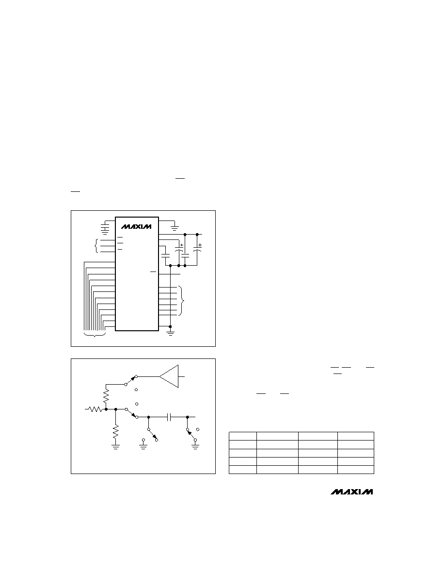
Digital Interface
Input data (control byte) and output data are multi-
plexed on a three-state parallel interface. This parallel
I/O can easily be interfaced with a P. CS, WR, and RD
control the write and read operations. CS is the stan-
dard chip-select signal, which enables a P to address
the MAX196/MAX198 as an I/O port. When high, it dis-
ables the WR and RD inputs and forces the interface
into a high-Z state.
DGND
VDD
REF
REFADJ
INT
CH5
CH4
CH3
CH2
CH1
CH0
AGND
28
27
23
4.7
F
4.7
F
0.01
F
0.01
F
+5V
OUTPUT STATUS
22
24
21
20
19
18
17
16
1
25
P
CONTROL
INPUTS
26
2
3
4
CLK
RD
WR
CS
D11
D10
D9
D8
D7
D6
D5
D4
D3
D2
D1
D0
100pF
P DATA BUS
15
5
6
7
8
9
10
11
12
13
14
ANALOG
INPUTS
MAX196
MAX198
Figure 3. Operational Diagram
5.12k
R2
R1
CH_
S1
S2
S3
S4
BIPOLAR
UNIPOLAR
VOLTAGE
REFERENCE
T/H
OUT
HOLD
TRACK
HOLD
OFF
ON
CHOLD
S1 = BIPOLAR/UNIPOLAR SWITCH
S2 = INPUT MUX SWITCH
S3, S4 = T/H SWITCH
R1 = 12.5k
(MAX196) OR 5.12k (MAX198)
R2 = 8.67k
(MAX196) OR ∞ (MAX198)
Figure 4. Equivalent Input Circuit
RANGE (V) ZERO SCALE (V) -FULL SCALE +FULL SCALE
0 to +5
0
—
VREF x 1.2207
0 to +10
0
—
VREF x 2.4414
±5
—
-VREF x 1.2207 VREF x 1.2207
±10
—
-VREF x 2.4414 VREF x 2.4414
Table 1. Full Scale and Zero Scale
(MAX196 only)
相关PDF资料 |
PDF描述 |
|---|---|
| VI-B50-MY-S | CONVERTER MOD DC/DC 5V 50W |
| VI-2TL-MY-S | CONVERTER MOD DC/DC 28V 50W |
| 74LCX138MTCX | DECODER/DEMUX 1OF8 16-TSSOP |
| D38999/26MJ19SA | CONN PLUG 19POS STRAIGHT W/SCKT |
| D38999/26MH53JN | CONN PLUG 53POS STRAIGHT W/SCKT |
相关代理商/技术参数 |
参数描述 |
|---|---|
| MAX196BCAI+ | 功能描述:模数转换器 - ADC 12-Bit 6Ch 100ksps 4.18V Precision ADC RoHS:否 制造商:Texas Instruments 通道数量:2 结构:Sigma-Delta 转换速率:125 SPs to 8 KSPs 分辨率:24 bit 输入类型:Differential 信噪比:107 dB 接口类型:SPI 工作电源电压:1.7 V to 3.6 V, 2.7 V to 5.25 V 最大工作温度:+ 85 C 安装风格:SMD/SMT 封装 / 箱体:VQFN-32 |
| MAX196BCAI+T | 功能描述:模数转换器 - ADC 12-Bit 6Ch 100ksps 4.18V Precision ADC RoHS:否 制造商:Texas Instruments 通道数量:2 结构:Sigma-Delta 转换速率:125 SPs to 8 KSPs 分辨率:24 bit 输入类型:Differential 信噪比:107 dB 接口类型:SPI 工作电源电压:1.7 V to 3.6 V, 2.7 V to 5.25 V 最大工作温度:+ 85 C 安装风格:SMD/SMT 封装 / 箱体:VQFN-32 |
| MAX196BCAI-T | 功能描述:模数转换器 - ADC RoHS:否 制造商:Texas Instruments 通道数量:2 结构:Sigma-Delta 转换速率:125 SPs to 8 KSPs 分辨率:24 bit 输入类型:Differential 信噪比:107 dB 接口类型:SPI 工作电源电压:1.7 V to 3.6 V, 2.7 V to 5.25 V 最大工作温度:+ 85 C 安装风格:SMD/SMT 封装 / 箱体:VQFN-32 |
| MAX196BCNI | 功能描述:模数转换器 - ADC Integrated Circuits (ICs) RoHS:否 制造商:Texas Instruments 通道数量:2 结构:Sigma-Delta 转换速率:125 SPs to 8 KSPs 分辨率:24 bit 输入类型:Differential 信噪比:107 dB 接口类型:SPI 工作电源电压:1.7 V to 3.6 V, 2.7 V to 5.25 V 最大工作温度:+ 85 C 安装风格:SMD/SMT 封装 / 箱体:VQFN-32 |
| MAX196BCNI+ | 功能描述:模数转换器 - ADC 12-Bit 6Ch 100ksps 4.18V Precision ADC RoHS:否 制造商:Texas Instruments 通道数量:2 结构:Sigma-Delta 转换速率:125 SPs to 8 KSPs 分辨率:24 bit 输入类型:Differential 信噪比:107 dB 接口类型:SPI 工作电源电压:1.7 V to 3.6 V, 2.7 V to 5.25 V 最大工作温度:+ 85 C 安装风格:SMD/SMT 封装 / 箱体:VQFN-32 |
发布紧急采购,3分钟左右您将得到回复。