- 您现在的位置:买卖IC网 > PDF目录9507 > MAX196BCAI+ (Maxim Integrated Products)IC DAS 6CH 12BIT 5V 28-SSOP PDF资料下载
参数资料
| 型号: | MAX196BCAI+ |
| 厂商: | Maxim Integrated Products |
| 文件页数: | 3/16页 |
| 文件大小: | 0K |
| 描述: | IC DAS 6CH 12BIT 5V 28-SSOP |
| 产品培训模块: | Lead (SnPb) Finish for COTS Obsolescence Mitigation Program |
| 标准包装: | 46 |
| 类型: | 数据采集系统(DAS) |
| 分辨率(位): | 12 b |
| 采样率(每秒): | 100k |
| 数据接口: | 并联 |
| 电压电源: | 单电源 |
| 电源电压: | 4.75 V ~ 5.25 V |
| 工作温度: | 0°C ~ 70°C |
| 安装类型: | 表面贴装 |
| 封装/外壳: | 28-SSOP(0.209",5.30mm 宽) |
| 供应商设备封装: | 28-SSOP |
| 包装: | 管件 |
| 产品目录页面: | 1393 (CN2011-ZH PDF) |
Clock Modes
The MAX196/MAX198 operate with either an internal or
an external clock. Control bits (D6, D7) select either
internal or external clock mode. Once the desired clock
mode is selected, changing these bits to program
power-down will not affect the clock mode. In each
mode, internal or external acquisition can be used. At
power-up, external clock mode is selected.
Internal Clock Mode
Select internal clock mode to free the P from the
burden of running the SAR conversion clock. To select
this mode, write the control byte with D7 = 0 and D6 =
1. A 100pF capacitor between the CLK pin and ground
sets this frequency to 1.56MHz nominal. Figure 7
shows a linear relationship between the internal clock
period and the value of the external capacitor used.
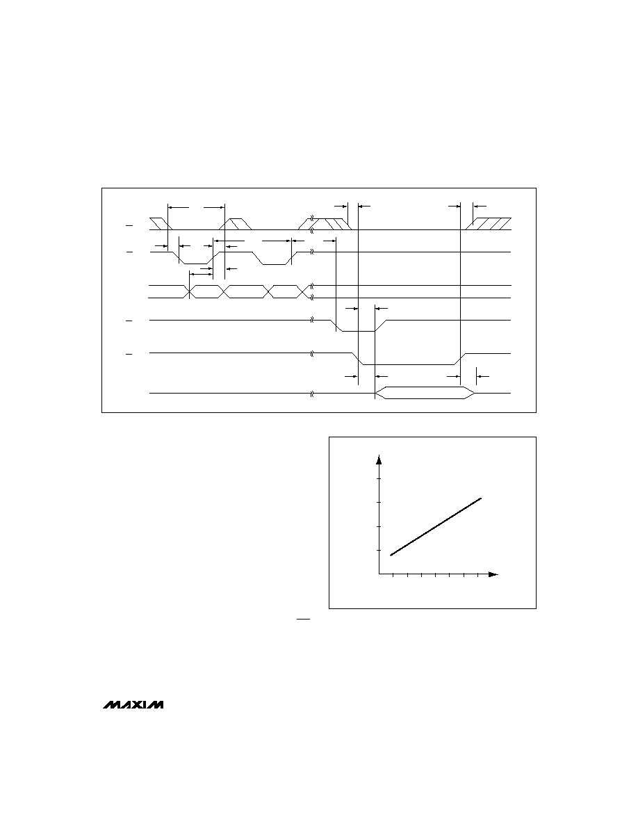
External Clock Mode
Select external clock mode by writing the control byte
with D7 = 0 and D6 = 0. Figure 8 shows CLK and WR
timing relationships in internal and external acquisition
modes, with an external clock. A 100kHz to 2.0MHz
external clock with 45% to 55% duty cycle is required for
proper operation. Operating at clock frequencies lower
than 100kHz will cause a voltage droop across the hold
capacitor, and subsequently degrade performance.
MAX196/MAX198
Multirange, Single +5V, 12-Bit DAS
with 12-Bit Bus Interface
______________________________________________________________________________________
11
tCS
tCSWS
tWR
tACQI
tCONV
tDH
tDS
tINT1
tD0
tTR
tCSHW
tCSRS
tCSRH
ACQMOD = "1"
CS
WR
D7–D0
INT
RD
DOUT
ACQMOD = "0"
DATA VALID
CONTROL
BYTE
CONTROL
BYTE
Figure 6. Conversion Timing Using External Acquisition Mode
2000
0
50
250
350
500
CLOCK PIN CAPACITANCE (pF)
INTERNAL
CLOCK
PERIOD
(ns)
100
150 200
300
1500
1000
Figure 7. Internal Clock Period vs. Clock Pin Capacitance
相关PDF资料 |
PDF描述 |
|---|---|
| VI-B50-MY-S | CONVERTER MOD DC/DC 5V 50W |
| VI-2TL-MY-S | CONVERTER MOD DC/DC 28V 50W |
| 74LCX138MTCX | DECODER/DEMUX 1OF8 16-TSSOP |
| D38999/26MJ19SA | CONN PLUG 19POS STRAIGHT W/SCKT |
| D38999/26MH53JN | CONN PLUG 53POS STRAIGHT W/SCKT |
相关代理商/技术参数 |
参数描述 |
|---|---|
| MAX196BCAI+ | 功能描述:模数转换器 - ADC 12-Bit 6Ch 100ksps 4.18V Precision ADC RoHS:否 制造商:Texas Instruments 通道数量:2 结构:Sigma-Delta 转换速率:125 SPs to 8 KSPs 分辨率:24 bit 输入类型:Differential 信噪比:107 dB 接口类型:SPI 工作电源电压:1.7 V to 3.6 V, 2.7 V to 5.25 V 最大工作温度:+ 85 C 安装风格:SMD/SMT 封装 / 箱体:VQFN-32 |
| MAX196BCAI+T | 功能描述:模数转换器 - ADC 12-Bit 6Ch 100ksps 4.18V Precision ADC RoHS:否 制造商:Texas Instruments 通道数量:2 结构:Sigma-Delta 转换速率:125 SPs to 8 KSPs 分辨率:24 bit 输入类型:Differential 信噪比:107 dB 接口类型:SPI 工作电源电压:1.7 V to 3.6 V, 2.7 V to 5.25 V 最大工作温度:+ 85 C 安装风格:SMD/SMT 封装 / 箱体:VQFN-32 |
| MAX196BCAI-T | 功能描述:模数转换器 - ADC RoHS:否 制造商:Texas Instruments 通道数量:2 结构:Sigma-Delta 转换速率:125 SPs to 8 KSPs 分辨率:24 bit 输入类型:Differential 信噪比:107 dB 接口类型:SPI 工作电源电压:1.7 V to 3.6 V, 2.7 V to 5.25 V 最大工作温度:+ 85 C 安装风格:SMD/SMT 封装 / 箱体:VQFN-32 |
| MAX196BCNI | 功能描述:模数转换器 - ADC Integrated Circuits (ICs) RoHS:否 制造商:Texas Instruments 通道数量:2 结构:Sigma-Delta 转换速率:125 SPs to 8 KSPs 分辨率:24 bit 输入类型:Differential 信噪比:107 dB 接口类型:SPI 工作电源电压:1.7 V to 3.6 V, 2.7 V to 5.25 V 最大工作温度:+ 85 C 安装风格:SMD/SMT 封装 / 箱体:VQFN-32 |
| MAX196BCNI+ | 功能描述:模数转换器 - ADC 12-Bit 6Ch 100ksps 4.18V Precision ADC RoHS:否 制造商:Texas Instruments 通道数量:2 结构:Sigma-Delta 转换速率:125 SPs to 8 KSPs 分辨率:24 bit 输入类型:Differential 信噪比:107 dB 接口类型:SPI 工作电源电压:1.7 V to 3.6 V, 2.7 V to 5.25 V 最大工作温度:+ 85 C 安装风格:SMD/SMT 封装 / 箱体:VQFN-32 |
发布紧急采购,3分钟左右您将得到回复。