- 您现在的位置:买卖IC网 > PDF目录10741 > MAX19705ETM+T (Maxim Integrated Products)IC ANLG FRNT END 48-TQFN PDF资料下载
参数资料
| 型号: | MAX19705ETM+T |
| 厂商: | Maxim Integrated Products |
| 文件页数: | 7/37页 |
| 文件大小: | 0K |
| 描述: | IC ANLG FRNT END 48-TQFN |
| 产品培训模块: | Lead (SnPb) Finish for COTS Obsolescence Mitigation Program |
| 标准包装: | 2,500 |
| 位数: | 10 |
| 通道数: | 4 |
| 功率(瓦特): | 28.2mW |
| 电压 - 电源,模拟: | 2.7 V ~ 3.3 V |
| 电压 - 电源,数字: | 1.8 V ~ 3.3 V |
| 封装/外壳: | 48-WFQFN 裸露焊盘 |
| 供应商设备封装: | 48-TQFN-EP(7x7) |
| 包装: | 带卷 (TR) |
第1页第2页第3页第4页第5页第6页当前第7页第8页第9页第10页第11页第12页第13页第14页第15页第16页第17页第18页第19页第20页第21页第22页第23页第24页第25页第26页第27页第28页第29页第30页第31页第32页第33页第34页第35页第36页第37页
MAX19705
10-Bit, 7.5Msps, Ultra-Low-Power
Analog Front-End
______________________________________________________________________________________
15
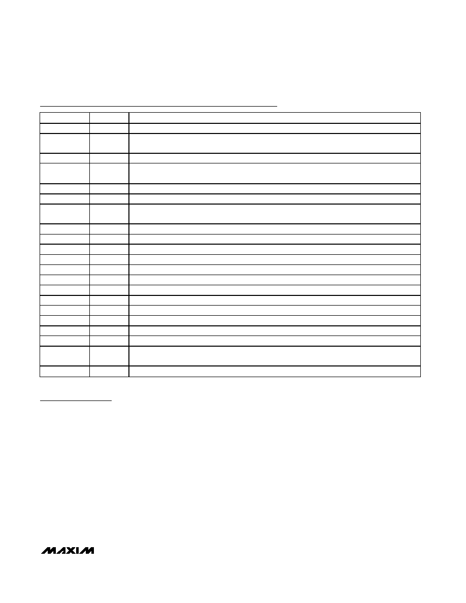
PIN
NAME
FUNCTION
10
QAP
Channel-QA Positive Analog Input. For single-ended operation, connect signal source to QAP.
13–18, 21–24
D0–D9
Digital I/O. Outputs for receive ADC in Rx mode. Inputs for transmit DAC in Tx mode. D9 is the most
significant bit (MSB) and D0 is the least significant bit (LSB).
19
OGND
Output-Driver Ground
20
OVDD
Output-Driver Power Supply. Supply range from +1.8V to VDD. Bypass OVDD to OGND with a
combination of a 2.2F capacitor in parallel with a 0.1F capacitor.
25
SHDN
Active-Low Shutdown Input. Apply logic-low to place the MAX19705 in shutdown.
26
DOUT
Aux-ADC Digital Output
27
T/R
Transmit- or Receive-Mode Select Input. T/R logic-low input sets the device in receive mode. A
logic-high input sets the device in transmit mode.
28
DIN
3-Wire Serial-Interface Data Input. Data is latched on the rising edge of the SCLK.
29
SCLK
3-Wire Serial-Interface Clock Input
30
CS
3-Wire Serial-Interface Chip-Select Input. Logic-low enables the serial interface.
34
ADC2
Analog Input for Auxiliary ADC
35
ADC1
Analog Input for Auxiliary ADC
36
DAC3
Analog Output for Auxiliary DAC3
37
DAC2
Analog Output for Auxiliary DAC2
38
DAC1
Analog Output for Auxiliary DAC1 (AFC DAC, VOUT = 1.1V During Power-Up)
40, 41
IDN, IDP
DAC Channel-ID Differential Voltage Output
44, 45
QDN, QDP
DAC Channel-QD Differential Voltage Output
46
REFIN
Reference Input. Connect to VDD for internal reference.
47
COM
Common-Mode Voltage I/O. Bypass COM to GND with a 0.33F capacitor.
48
REFN
Negative Reference I/O. Rx ADC conversion range is ±(VREFP - VREFN). Bypass REFN to GND with a
0.1F capacitor.
—EPExposed Paddle. Exposed paddle is internally connected to GND. Connect EP to the GND plane.
Pin Description (continued)
SPI is a trademark of Motorola, Inc.
MICROWIRE is a trademark of National Semiconductor Corp.
Detailed Description
The MAX19705 integrates a dual 10-bit Rx ADC and a
dual 10-bit Tx DAC while providing ultra-low power and
high dynamic performance at 7.5Msps conversion rate.
The Rx ADC analog input amplifiers are fully differential
and accept 1.024VP-P full-scale signals. The Tx DAC
analog outputs are fully differential with ±400mV full-
scale output, selectable common-mode DC level, and
adjustable I/Q offset trim.
The MAX19705 integrates three 12-bit auxiliary DAC
(aux-DAC) channels and a 10-bit, 333ksps auxiliary
ADC (aux-ADC) with 4:1 input multiplexer. The aux-DAC
channels feature 1s settling time for fast AGC, VGA,
and AFC level setting. The aux-ADC features data aver-
aging to reduce processor overhead and a selectable
clock-divider to program the conversion rate.
The MAX19705 includes a 3-wire serial interface to
control operating modes and power management. The
serial interface is SPI and MICROWIRE compatible.
The MAX19705 serial interface selects shutdown, idle,
standby, transmit (Tx), and receive (Rx) modes, as well
as controlling aux-DAC and aux-ADC channels.
The Rx ADC and Tx DAC share a common digital I/O to
reduce the digital interface to a single 10-bit parallel
multiplexed bus. The 10-bit digital bus operates on a
single +1.8V to +3.3V supply.
相关PDF资料 |
PDF描述 |
|---|---|
| MAX978ESE+ | IC COMPARATOR QUAD 16-SOIC |
| MAX5866ETM+T | IC ANLG FRONT END 60MSPS 48-TQFN |
| MAX978EEE+ | IC COMPARATOR QUAD 16-QSOP |
| MAX913CPA+ | IC COMPARATOR TTL SNGL HS 8-DIP |
| ISL98002CRZ-140 | IC VID DIGITIZER 3CHN AFE 72-QFN |
相关代理商/技术参数 |
参数描述 |
|---|---|
| MAX19705EVCMOD2 | 功能描述:ADC / DAC多通道 Evaluation System for the MAX19705 RoHS:否 制造商:Texas Instruments 转换速率: 分辨率:8 bit 接口类型:SPI 电压参考: 电源电压-最大:3.6 V 电源电压-最小:2 V 最大工作温度:+ 85 C 安装风格:SMD/SMT 封装 / 箱体:VQFN-40 |
| MAX19705EVCMODU | 功能描述:ADC / DAC多通道 Evaluation System for the MAX19705 RoHS:否 制造商:Texas Instruments 转换速率: 分辨率:8 bit 接口类型:SPI 电压参考: 电源电压-最大:3.6 V 电源电压-最小:2 V 最大工作温度:+ 85 C 安装风格:SMD/SMT 封装 / 箱体:VQFN-40 |
| MAX19705EVKIT | 功能描述:数据转换 IC 开发工具 Evaluation Kit for the MAX19705 MAX19706 MAX19707 MAX19708 RoHS:否 制造商:Texas Instruments 产品:Demonstration Kits 类型:ADC 工具用于评估:ADS130E08 接口类型:SPI 工作电源电压:- 6 V to + 6 V |
| MAX19706ETM | 功能描述:ADC / DAC多通道 RoHS:否 制造商:Texas Instruments 转换速率: 分辨率:8 bit 接口类型:SPI 电压参考: 电源电压-最大:3.6 V 电源电压-最小:2 V 最大工作温度:+ 85 C 安装风格:SMD/SMT 封装 / 箱体:VQFN-40 |
| MAX19706ETM+ | 功能描述:ADC / DAC多通道 22Msps CODEC/AFE 1.8/2.7-3.3V RoHS:否 制造商:Texas Instruments 转换速率: 分辨率:8 bit 接口类型:SPI 电压参考: 电源电压-最大:3.6 V 电源电压-最小:2 V 最大工作温度:+ 85 C 安装风格:SMD/SMT 封装 / 箱体:VQFN-40 |
发布紧急采购,3分钟左右您将得到回复。