- 您现在的位置:买卖IC网 > PDF目录9459 > MAX197AEWI+T (Maxim Integrated Products)IC DAS 12BIT SNGL 28-SOIC PDF资料下载
参数资料
| 型号: | MAX197AEWI+T |
| 厂商: | Maxim Integrated Products |
| 文件页数: | 16/16页 |
| 文件大小: | 0K |
| 描述: | IC DAS 12BIT SNGL 28-SOIC |
| 产品培训模块: | Lead (SnPb) Finish for COTS Obsolescence Mitigation Program |
| 标准包装: | 1,000 |
| 类型: | 数据采集系统(DAS) |
| 分辨率(位): | 12 b |
| 采样率(每秒): | 100k |
| 数据接口: | 并联 |
| 电压电源: | 单电源 |
| 电源电压: | 4.75 V ~ 5.25 V |
| 工作温度: | -40°C ~ 85°C |
| 安装类型: | 表面贴装 |
| 封装/外壳: | 28-SOIC(0.295",7.50mm 宽) |
| 供应商设备封装: | 28-SOIC W |
| 包装: | 带卷 (TR) |
The input channels are overvoltage protected to
±16.5V. This protection is active even if the device is in
power-down mode.
Even with VDD = 0V, the input resistive network provides
current-limiting that adequately protects the device.
Digital Interface
Input data (control byte) and output data are multiplexed
on a three-state parallel interface. This parallel I/O can
easily be interfaced with a P. CS, WR, and RD control
the write and read operations. CS is the standard chip-
select signal, which enables a P to address the MAX197
as an I/O port. When high, it disables the WR and RD
inputs and forces the interface into a high-Z state.
Input Format
The control byte is latched into the device, on pins
D7–D0, during a write cycle. Table 2 shows the control-
byte format.
Output Data Format
The output data format is binary in unipolar mode and
twos-complement binary in bipolar mode. When read-
ing the output data, CS, and RD must be low. When
HBEN is low, the lower eight bits are read. When HBEN
is high, the upper four MSBs are available and the out-
put data bits D4–D7 are either set low (in unipolar
mode) or set to the value of the MSB (in bipolar mode)
(Table 6).
MAX197
Multi-Range (±10V, ±5V, +10V, +5V),
Single +5V, 12-Bit DAS with 8+4 Bus Interface
_______________________________________________________________________________________
9
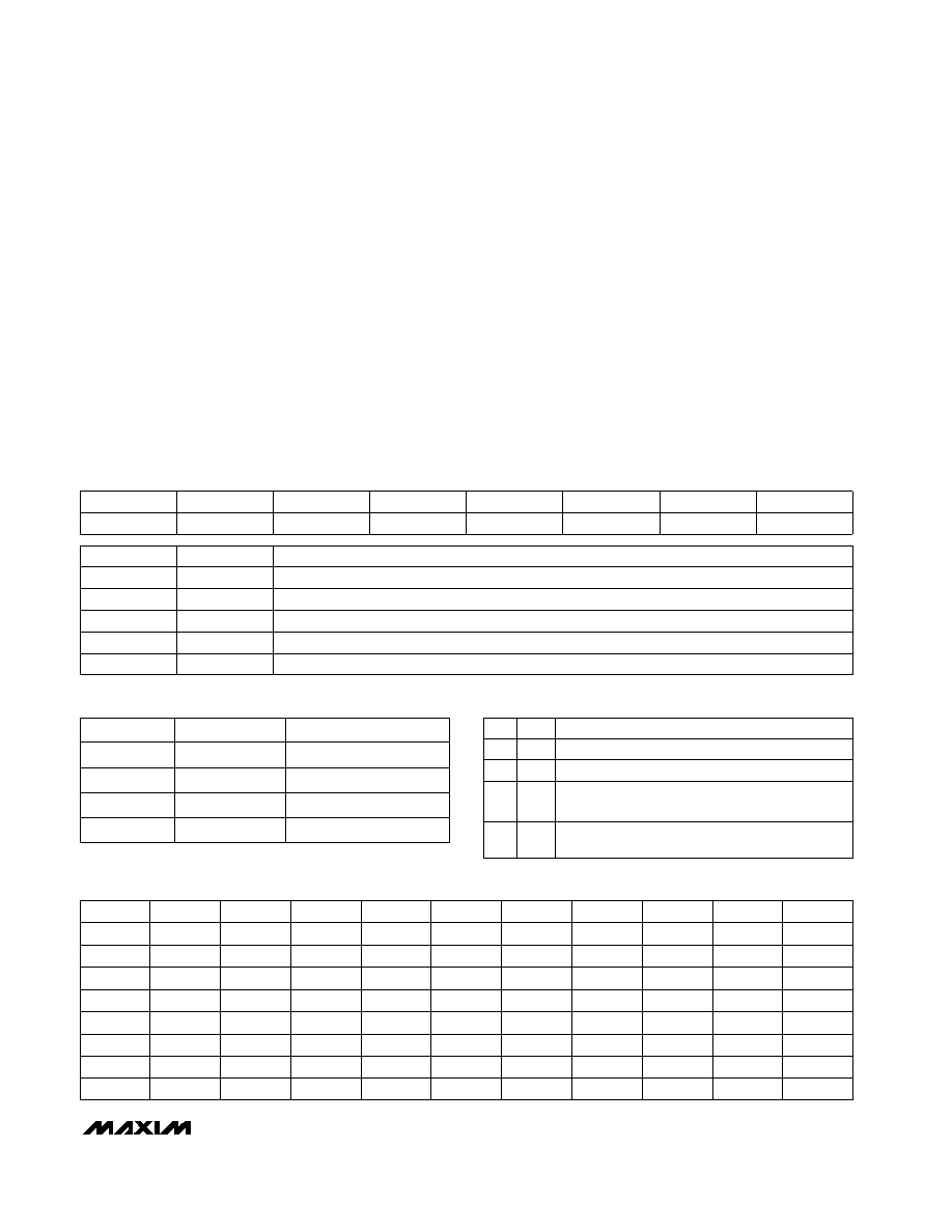
Table 2. Control-Byte Format
D7 (MSB)
D6
D5
D4
D3
D2
D1
D0 (LSB)
PD1
PD0
ACQMOD
RNG
BIP
A2
A1
A0
Table 4. Clock and Power-Down Selection
PD1 PD0
DEVICE MODE
0
Normal Operation / External Clock Mode
0
1
Normal Operation / Internal Clock Mode
1
0
Standby Power-Down (STBYPD); clock mode
is unaffected
1
Full Power-Down (FULLPD); clock mode is
unaffected
Table 3. Range and Polarity Selection
BIP
RNG
INPUT RANGE (V)
0
0 to 5
0
1
0 to 10
1
0
±5
1
±10
Table 5. Channel Selection
A2
A1
A0
CH0
CH1
CH2
CH3
CH4
CH5
CH6
CH7
0
—
0
1
—
0
1
0
—
0
1
—
1
0
—
1
0
1
—
1
0
—
1
—
BIT
NAME
DESCRIPTION
7, 6
PD1, PD0
These two bits select the clock and power-down modes (Table 4).
5
ACQMOD
0 = internally controlled acquisition (6 clock cycles), 1 = externally controlled acquisition
4
RNG
Selects the full-scale voltage magnitude at the input (Table 3).
3
BIP
Selects unipolar or bipolar conversion mode (Table 3).
2, 1, 0
A2, A1, A0
These are address bits for the input mux to select the “on” channel (Table 5).
相关PDF资料 |
PDF描述 |
|---|---|
| VI-B14-MX-B1 | CONVERTER MOD DC/DC 48V 75W |
| MAX198AEWI+T | IC DAS 12BIT 6CH 28-SOIC |
| MAX188CEAP+ | IC ADC 12BIT SERIAL 20-SSOP |
| VE-BWX-MX-B1 | CONVERTER MOD DC/DC 5.2V 75W |
| VE-BW0-MX-B1 | CONVERTER MOD DC/DC 5V 75W |
相关代理商/技术参数 |
参数描述 |
|---|---|
| MAX197AMWI/PR | 制造商:Maxim Integrated Products 功能描述:- Rail/Tube |
| MAX197AMYI | 功能描述:模数转换器 - ADC RoHS:否 制造商:Texas Instruments 通道数量:2 结构:Sigma-Delta 转换速率:125 SPs to 8 KSPs 分辨率:24 bit 输入类型:Differential 信噪比:107 dB 接口类型:SPI 工作电源电压:1.7 V to 3.6 V, 2.7 V to 5.25 V 最大工作温度:+ 85 C 安装风格:SMD/SMT 封装 / 箱体:VQFN-32 |
| MAX197BC/D | 功能描述:模数转换器 - ADC RoHS:否 制造商:Texas Instruments 通道数量:2 结构:Sigma-Delta 转换速率:125 SPs to 8 KSPs 分辨率:24 bit 输入类型:Differential 信噪比:107 dB 接口类型:SPI 工作电源电压:1.7 V to 3.6 V, 2.7 V to 5.25 V 最大工作温度:+ 85 C 安装风格:SMD/SMT 封装 / 箱体:VQFN-32 |
| MAX197BCAI | 功能描述:模数转换器 - ADC Integrated Circuits (ICs) RoHS:否 制造商:Texas Instruments 通道数量:2 结构:Sigma-Delta 转换速率:125 SPs to 8 KSPs 分辨率:24 bit 输入类型:Differential 信噪比:107 dB 接口类型:SPI 工作电源电压:1.7 V to 3.6 V, 2.7 V to 5.25 V 最大工作温度:+ 85 C 安装风格:SMD/SMT 封装 / 箱体:VQFN-32 |
| MAX197BCAI+ | 功能描述:模数转换器 - ADC 12-Bit 8Ch 100ksps 4.18V Precision ADC RoHS:否 制造商:Texas Instruments 通道数量:2 结构:Sigma-Delta 转换速率:125 SPs to 8 KSPs 分辨率:24 bit 输入类型:Differential 信噪比:107 dB 接口类型:SPI 工作电源电压:1.7 V to 3.6 V, 2.7 V to 5.25 V 最大工作温度:+ 85 C 安装风格:SMD/SMT 封装 / 箱体:VQFN-32 |
发布紧急采购,3分钟左右您将得到回复。