- 您现在的位置:买卖IC网 > PDF目录9459 > MAX197AEWI+T (Maxim Integrated Products)IC DAS 12BIT SNGL 28-SOIC PDF资料下载
参数资料
| 型号: | MAX197AEWI+T |
| 厂商: | Maxim Integrated Products |
| 文件页数: | 3/16页 |
| 文件大小: | 0K |
| 描述: | IC DAS 12BIT SNGL 28-SOIC |
| 产品培训模块: | Lead (SnPb) Finish for COTS Obsolescence Mitigation Program |
| 标准包装: | 1,000 |
| 类型: | 数据采集系统(DAS) |
| 分辨率(位): | 12 b |
| 采样率(每秒): | 100k |
| 数据接口: | 并联 |
| 电压电源: | 单电源 |
| 电源电压: | 4.75 V ~ 5.25 V |
| 工作温度: | -40°C ~ 85°C |
| 安装类型: | 表面贴装 |
| 封装/外壳: | 28-SOIC(0.295",7.50mm 宽) |
| 供应商设备封装: | 28-SOIC W |
| 包装: | 带卷 (TR) |
How to Read a Conversion
A standard interrupt signal, INT, is provided to allow the
device to flag the P when the conversion has ended
and a valid result is available. INT goes low when con-
version is complete and the output data is ready
(Figures 5 and 6). It returns high on the first read cycle
or if a new control byte is written.
Clock Modes
The MAX197 operates with either an internal or an
external clock. Control bits (D6, D7) select either inter-
nal or external clock mode. Once the desired clock
mode is selected, changing these bits to program
power-down will not affect the clock mode. In each
mode, internal or external acquisition can be used. At
power-up, external clock mode is selected.
Internal Clock Mode
Select internal clock mode to free the P from the
burden of running the SAR conversion clock. To select
this mode, write the control byte with D7 = 0 and D6 = 1.
A 100pF capacitor between the CLK pin and ground
sets this frequency to 1.56MHz nominal. Figure 7
shows a linear relationship between the internal clock
period and the value of the external capacitor used.
MAX197
Multi-Range (±10V, ±5V, +10V, +5V),
Single +5V, 12-Bit DAS with 8+4 Bus Interface
______________________________________________________________________________________
11
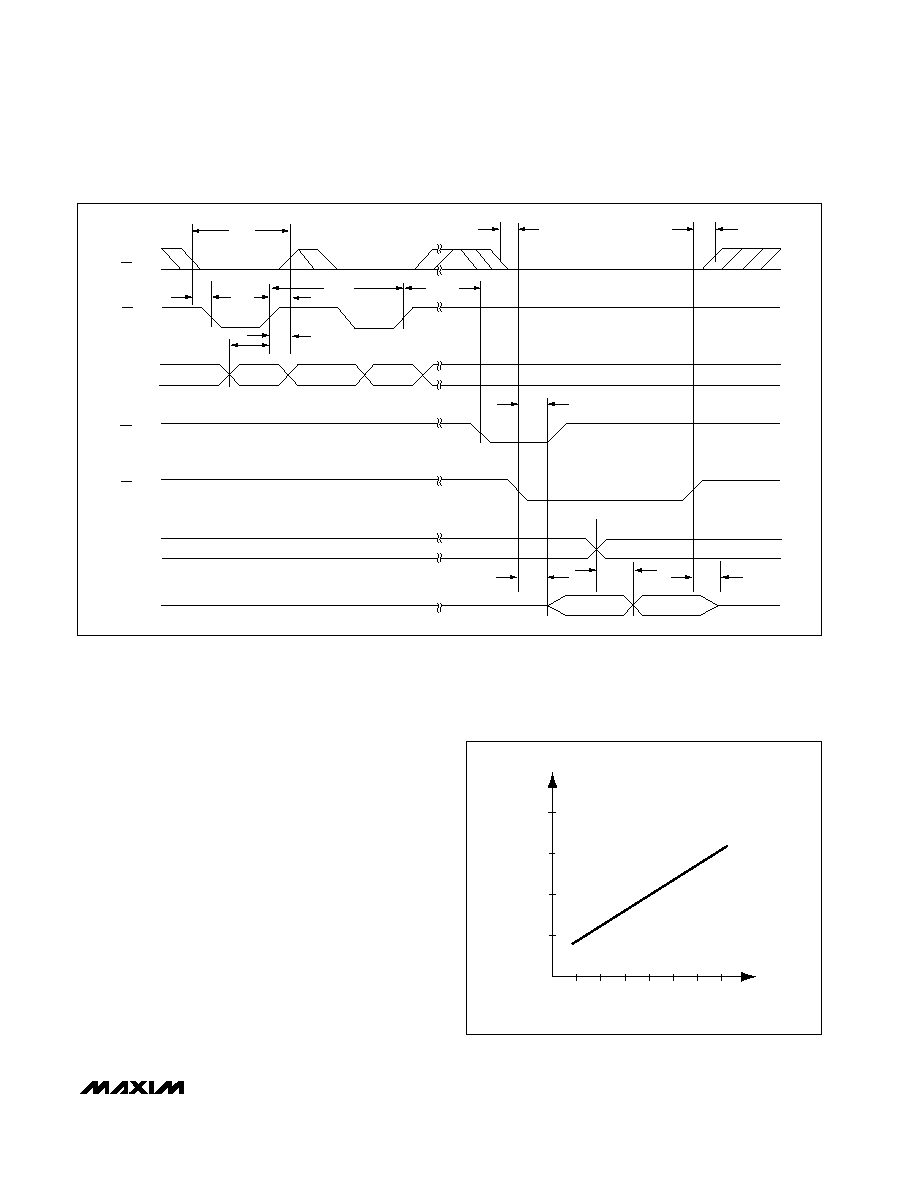
tCS
tCSWS
tWR
tACQI
tCONV
tDH
tDS
tINT1
tD0
tD01
tTR
tCSHW
tCSRS
tCSRH
ACQMOD = "1"
CS
WR
D7–D0
INT
RD
HBEN
DOUT
ACQMOD = "0"
HIGH / LOW
BYTE VALID
HIGH / LOW
BYTE VALID
CONTROL
BYTE
CONTROL
BYTE
Figure 6. Conversion Timing Using External Acquisition Mode
2000
0
50
250
350
500
CLOCK PIN CAPACITANCE (pF)
INTERNAL
CLOCK
PERIOD
(ns)
100
150 200
300
1500
1000
Figure 7. Internal Clock Period vs. Clock Pin Capacitance
相关PDF资料 |
PDF描述 |
|---|---|
| VI-B14-MX-B1 | CONVERTER MOD DC/DC 48V 75W |
| MAX198AEWI+T | IC DAS 12BIT 6CH 28-SOIC |
| MAX188CEAP+ | IC ADC 12BIT SERIAL 20-SSOP |
| VE-BWX-MX-B1 | CONVERTER MOD DC/DC 5.2V 75W |
| VE-BW0-MX-B1 | CONVERTER MOD DC/DC 5V 75W |
相关代理商/技术参数 |
参数描述 |
|---|---|
| MAX197AMWI/PR | 制造商:Maxim Integrated Products 功能描述:- Rail/Tube |
| MAX197AMYI | 功能描述:模数转换器 - ADC RoHS:否 制造商:Texas Instruments 通道数量:2 结构:Sigma-Delta 转换速率:125 SPs to 8 KSPs 分辨率:24 bit 输入类型:Differential 信噪比:107 dB 接口类型:SPI 工作电源电压:1.7 V to 3.6 V, 2.7 V to 5.25 V 最大工作温度:+ 85 C 安装风格:SMD/SMT 封装 / 箱体:VQFN-32 |
| MAX197BC/D | 功能描述:模数转换器 - ADC RoHS:否 制造商:Texas Instruments 通道数量:2 结构:Sigma-Delta 转换速率:125 SPs to 8 KSPs 分辨率:24 bit 输入类型:Differential 信噪比:107 dB 接口类型:SPI 工作电源电压:1.7 V to 3.6 V, 2.7 V to 5.25 V 最大工作温度:+ 85 C 安装风格:SMD/SMT 封装 / 箱体:VQFN-32 |
| MAX197BCAI | 功能描述:模数转换器 - ADC Integrated Circuits (ICs) RoHS:否 制造商:Texas Instruments 通道数量:2 结构:Sigma-Delta 转换速率:125 SPs to 8 KSPs 分辨率:24 bit 输入类型:Differential 信噪比:107 dB 接口类型:SPI 工作电源电压:1.7 V to 3.6 V, 2.7 V to 5.25 V 最大工作温度:+ 85 C 安装风格:SMD/SMT 封装 / 箱体:VQFN-32 |
| MAX197BCAI+ | 功能描述:模数转换器 - ADC 12-Bit 8Ch 100ksps 4.18V Precision ADC RoHS:否 制造商:Texas Instruments 通道数量:2 结构:Sigma-Delta 转换速率:125 SPs to 8 KSPs 分辨率:24 bit 输入类型:Differential 信噪比:107 dB 接口类型:SPI 工作电源电压:1.7 V to 3.6 V, 2.7 V to 5.25 V 最大工作温度:+ 85 C 安装风格:SMD/SMT 封装 / 箱体:VQFN-32 |
发布紧急采购,3分钟左右您将得到回复。