- 您现在的位置:买卖IC网 > PDF目录18730 > MAX2031ETP+T (Maxim Integrated)IC MIXER UP/DWN HI LIN 20-TQFN PDF资料下载
参数资料
| 型号: | MAX2031ETP+T |
| 厂商: | Maxim Integrated |
| 文件页数: | 16/20页 |
| 文件大小: | 0K |
| 描述: | IC MIXER UP/DWN HI LIN 20-TQFN |
| 产品培训模块: | Lead (SnPb) Finish for COTS Obsolescence Mitigation Program |
| 标准包装: | 2,500 |
| 系列: | MAX2031 |
| RF 型: | 手机,CDMA2000,EDGE,GSM,W-CDMA |
| 频率: | 650MHz ~ 1GHz |
| 混频器数目: | 1 |
| 噪音数据: | 7dB |
| 次要属性: | 升/降频器 |
| 电流 - 电源: | 100mA |
| 电源电压: | 4.75 V ~ 5.25 V |
| 包装: | 带卷 (TR) |
| 封装/外壳: | 20-WQFN 裸露焊盘 |
| 供应商设备封装: | 20-TQFN-EP(5x5) |
�� �
�
�High-Linearity,� 650MHz� to� 1000MHz� Upconversion/�
�Downconversion� Mixer� with� LO� Buffer/Switch�
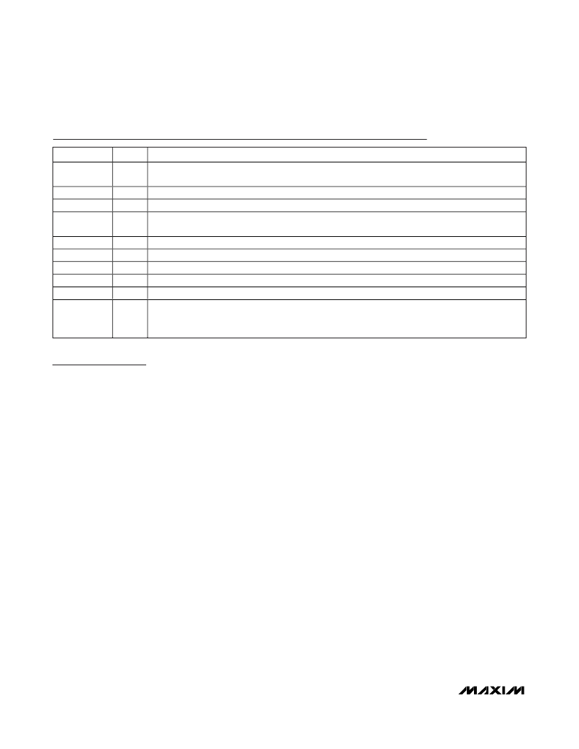
�Pin� Description�
�PIN�
�1,� 6,� 8,� 14�
�2�
�3�
�4,� 5,� 10,� 12,�
�13,� 16,� 17,� 20�
�NAME�
�V� CC�
�RF�
�TAP�
�GND�
�FUNCTION�
�Power-Supply� Connection.� Bypass� each� V� CC� pin� to� GND� with� capacitors� as� shown� in� the� Typical�
�Application� Circuit� .�
�Single-Ended 50� Ω� RF Input/Output. This port is internally matched and DC shorted to GND through a balun.�
�Center� Tap� of� the� Internal� RF� Balun.� Connect� to� ground.�
�Ground�
�7�
�LOBIAS� Bias� Resistor� for� Internal� LO� Buffer.� Connect� a� 523� Ω� ±1%� resistor� from� LOBIAS� to� the� power� supply.�
�9�
�11�
�15�
�18,� 19�
�—�
�LOSEL�
�LO1�
�LO2�
�IF-,� IF+�
�EP�
�Local� Oscillator� Select.� Logic-control� input� for� selecting� LO1� or� LO2.�
�Local� Oscillator� Input� 1.� Drive� LOSEL� low� to� select� LO1.�
�Local� Oscillator� Input� 2.� Drive� LOSEL� high� to� select� LO2.�
�Differential� IF� Input/Outputs�
�Exposed� Pad.� Internally� connected� to� GND.� Solder� this� exposed� pad� to� a� PCB� pad� that� uses� multiple�
�ground� vias� to� provide� heat� transfer� out� of� the� device� into� the� PCB� ground� planes.� These� multiple� ground�
�vias� are� also� required� to� achieve� the� noted� RF� performance.�
�Detailed� Description�
�The� MAX2031� can� operate� either� as� a� downconverter� or�
�an� upconverter� mixer� that� provides� approximately� 7dB� of�
�conversion� loss� with� a� typical� 7dB� noise� figure.� IIP3� is�
�+36dBm� for� both� upconversion� and� downconversion�
�modes.� The� integrated� baluns� and� matching� circuitry�
�allow� for� 50� Ω� single-ended� interfaces� to� the� RF� port� and�
�the� two� LO� ports.� The� RF� port� can� be� used� as� an� input�
�for� downconversion� or� an� output� for� upconversion.� A� sin-�
�gle-pole,� double-throw� (SPDT)� switch� provides� 50ns�
�switching� time� between� the� two� LO� inputs� with� 49dB� of�
�LO-to-LO� isolation.� Furthermore,� the� integrated� LO� buffer�
�provides� a� high� drive� level� to� the� mixer� core,� reducing�
�the� LO� drive� required� at� the� MAX2031� ’s� inputs� to� a�
�-3dBm� to� +3dBm� range.� The� IF� port� incorporates� a� dif-�
�ferential� output� for� downconversion,� which� is� ideal� for�
�providing� enhanced� IIP2� performance.� For� upconver-�
�sion,� the� IF� port� is� a� differential� input.�
�Specifications� are� guaranteed� over� broad� frequency�
�ranges� to� allow� for� use� in� cellular� band� WCDMA,�
�cdmaOne?,� cdma2000,� and� GSM� 850/GSM� 900� 2.5G�
�EDGE� base� stations.� The� MAX2031� is� specified� to� oper-�
�ate� over� a� 650MHz� to� 1000MHz� RF� frequency� range,� a�
�650MHz� to� 1250MHz� LO� frequency� range,� and� a� DC� to�
�250MHz� IF� frequency� range.� Operation� beyond� these�
�ranges� is� possible;� see� the� Typical� Operating�
�Characteristics� for� additional� details.�
�The� MAX2031� is� optimized� for� high-side� LO� injection�
�architectures.� However,� the� device� can� operate� in� low-�
�cdmaOne� is� a� trademark� of� CDMA� Development� Group.�
�side� LO� injection� applications� with� an� extended� LO�
�range,� but� performance� degrades� as� f� LO� decreases.� See�
�the� Typical� Operating� Characteristics� for� measurements�
�taken� with� f� LO� below� 960MHz.� For� a� pin-compatible�
�device� that� has� been� optimized� for� LO� frequencies� below�
�960MHz,� refer� to� the� MAX2029.�
�RF� Port� and� Balun�
�For� using� the� MAX2031� as� a� downconverter,� the� RF�
�input� is� internally� matched� to� 50� Ω� ,� requiring� no� external�
�matching� components.� A� DC-blocking� capacitor� is�
�required� because� the� input� is� internally� DC� shorted� to�
�ground� through� the� on-chip� balun.� For� upconverter�
�operation,� the� RF� port� is� a� single-ended� output� similarly�
�matched� to� 50� Ω� .�
�LO� Inputs,� Buffer,� and� Balun�
�The� MAX2031� is� optimized� for� high-side� LO� injection�
�architectures� with� a� 650MHz� to� 1250MHz� LO� frequency�
�range.� For� a� device� with� a� 570MHz� to� 900MHz� LO� fre-�
�quency� range,� refer� to� the� MAX2029.� As� an� added� fea-�
�ture,� the� MAX2031� includes� an� internal� LO� SPDT� switch�
�that� can� be� used� for� frequency-hopping� applications.�
�The� switch� selects� one� of� the� two� single-ended� LO�
�ports,� allowing� the� external� oscillator� to� settle� on� a� par-�
�ticular� frequency� before� it� is� switched� in.� LO� switching�
�time� is� typically� less� than� 50ns,� which� is� more� than� ade-�
�quate� for� nearly� all� GSM� applications.� If� frequency� hop-�
�ping� is� not� employed,� set� the� switch� to� either� of� the� LO�
�inputs.� The� switch� is� controlled� by� a� digital� input�
�(LOSEL):� logic-high� selects� LO2,� logic-low� selects� LO1.�
�16�
�______________________________________________________________________________________�
�相关PDF资料 |
PDF描述 |
|---|---|
| SST12LP14-QVCE | IC RF PWR AMP 802.11G 16-QFN |
| MAX2039ETP+T | IC MIXER UP/DWN HI LIN 20-TQFN |
| 636L3C029M49120 | OSCILLATOR 29.4912 MHZ 3.3V SMD |
| MAX2044ETP+ | IC MIXER UP/DOWN CONVER 20TQFN |
| SST12LP15A-QVCE | IC RF PWR AMP 802.11B/G/N 16-QFN |
相关代理商/技术参数 |
参数描述 |
|---|---|
| MAX2031EVKIT | 功能描述:射频混合器 RoHS:否 制造商:NXP Semiconductors 频率范围: 转换损失——最大: 工作电源电压:6 V 最大工作温度:+ 85 C 最小工作温度:- 40 C 安装风格:Through Hole 封装 / 箱体:PDIP-8 封装:Tube |
| MAX2032 | 制造商:MAXIM 制造商全称:Maxim Integrated Products 功能描述:High-Linearity, 650MHz to 1000MHz Upconversion/Downconversion Mixer with LO Buffer/Switch |
| MAX2032ETP+ | 功能描述:射频混合器 .65GHz-1GHz Up/Down Mixer RoHS:否 制造商:NXP Semiconductors 频率范围: 转换损失——最大: 工作电源电压:6 V 最大工作温度:+ 85 C 最小工作温度:- 40 C 安装风格:Through Hole 封装 / 箱体:PDIP-8 封装:Tube |
| MAX2032ETP+T | 功能描述:射频混合器 .65GHz-1GHz Up/Down Mixer RoHS:否 制造商:NXP Semiconductors 频率范围: 转换损失——最大: 工作电源电压:6 V 最大工作温度:+ 85 C 最小工作温度:- 40 C 安装风格:Through Hole 封装 / 箱体:PDIP-8 封装:Tube |
| MAX2034 | 制造商:MAXIM 制造商全称:Maxim Integrated Products 功能描述:Quad-Channel, Ultra-Low-Noise Amplifier with Digitally Programmable Input Impedance |
发布紧急采购,3分钟左右您将得到回复。