- 您现在的位置:买卖IC网 > Datasheet目录471 > MAX2032ETP+ (Maxim Integrated)IC MIXER UP/DOWN CONVER 20TQFN Datasheet资料下载
参数资料
| 型号: | MAX2032ETP+ |
| 厂商: | Maxim Integrated |
| 文件页数: | 2/19页 |
| 文件大小: | 0K |
| 描述: | IC MIXER UP/DOWN CONVER 20TQFN |
| 产品培训模块: | Lead (SnPb) Finish for COTS Obsolescence Mitigation Program |
| 标准包装: | 60 |
| RF 型: | GSM,EDGE,CDMA |
| 频率: | 650MHz ~ 1GHz |
| 混频器数目: | 1 |
| 噪音数据: | 7dB |
| 次要属性: | 升/降频器 |
| 电流 - 电源: | 85mA |
| 电源电压: | 4.75 V ~ 5.25 V |
| 包装: | 管件 |
| 封装/外壳: | 20-WQFN 裸露焊盘 |
| 供应商设备封装: | 20-TQFN-EP(5x5) |
�� �
�
�High-Linearity,� 650MHz� to� 1000MHz� Upconversion/�
�Downconversion� Mixer� with� LO� Buffer/Switch�
�ABSOLUTE� MAXIMUM� RATINGS�
�V� CC� to� GND� ...........................................................-0.3V� to� +5.5V�
�RF� (RF� is� DC� shorted� to� GND� through� a� balun)..................50mA�
�LO1,� LO2� to� GND� ..................................................-0.3V� to� +0.3V�
�IF+,� IF-� to� GND� ...........................................-0.3V� to� (V� CC� +� 0.3V)�
�TAP� to� GND� ...........................................................-0.3V� to� +1.4V�
�LOSEL� to� GND� ...........................................-0.3V� to� (V� CC� +� 0.3V)�
�LOBIAS� to� GND..........................................-0.3V� to� (V� CC� +� 0.3V)�
�Continuous� Power� Dissipation� (Note� 2)....................................5W�
�θ� JA� (Notes� 3,� 4)..............................................................+38°C/W�
�θ� JC� (Notes� 2,� 3)..............................................................+13°C/W�
�Operating� Temperature� Range� (Note� 5)� .....T� C� =� -40°C� to� +85°C�
�Junction� Temperature� ......................................................+150°C�
�Storage� Temperature� Range� .............................-65°C� to� +150°C�
�Lead� Temperature� (soldering,� 10s)� .................................+300°C�
�RF,� LO1,� LO2� Input� Power� (Note� 1)� ...............................+20dBm�
�Note� 1:� Maximum,� reliable,� continuous� input� power� applied� to� the� RF� and� IF� port� of� this� device� is� +12dBm� from� a� 50� ?� source.�
�Note� 2:� Based� on� junction� temperature� T� J� =� T� C� +� (� θ� JC� x� V� CC� x� I� CC� ).� This� formula� can� be� used� when� the� temperature� of� the� exposed�
�pad� is� known� while� the� device� is� soldered� down� to� a� PCB.� See� the� Applications� Information� section� for� details.� The� junction�
�temperature� must� not� exceed� +150°C.�
�Note� 3:� Package� thermal� resistances� were� obtained� using� the� method� described� in� JEDEC� specification� JESD51-7,� using� a� four-�
�layer� board.� For� detailed� information� on� package� thermal� considerations,� refer� to� www.maxim-ic.com/thermal-tutorial� .�
�Note� 4:� Junction� temperature� T� J� =� T� A� +� (� θ� JA� x� V� CC� x� I� CC� ).� This� formula� can� be� used� when� the� ambient� temperature� of� the� PCB� is�
�known.� The� junction� temperature� must� not� exceed� +150°C.�
�Note� 5:� T� C� is� the� temperature� on� the� exposed� pad� of� the� package.� T� A� is� the� ambient� temperature� of� the� device� and� PCB.�
�Stresses� beyond� those� listed� under� “Absolute� Maximum� Ratings”� may� cause� permanent� damage� to� the� device.� These� are� stress� ratings� only,� and� functional�
�operation� of� the� device� at� these� or� any� other� conditions� beyond� those� indicated� in� the� operational� sections� of� the� specifications� is� not� implied.� Exposure� to�
�absolute� maximum� rating� conditions� for� extended� periods� may� affect� device� reliability.�
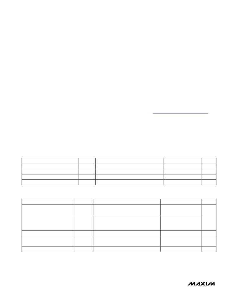
�DC� ELECTRICAL� CHARACTERISTICS�
�(Typical� Application� Circuit,� V� CC� =� 4.75V� to� 5.25V,� no� RF� signals� applied,� T� C� =� -40°C� to� +85°C.� IF+� and� IF-� are� DC� grounded� through� an�
�IF� balun.� Typical� values� are� at� V� CC� =� 5V,� T� C� =� +25°C,� unless� otherwise� noted.)�
�PARAMETER�
�Supply� Voltage�
�Supply� Current�
�SYMBOL�
�V� CC�
�I� CC�
�CONDITIONS�
�MIN�
�4.75�
�TYP�
�5.00�
�85�
�MAX�
�5.25�
�100�
�UNITS�
�V�
�mA�
�LOSEL� Input� Logic-Low�
�LOSEL� Input� Logic-High�
�V� IL�
�V� IH�
�2�
�0.8�
�V�
�V�
�RECOMMENDED� AC� OPERATING� CONDITIONS�
�PARAMETER�
�SYMBOL�
�CONDITIONS�
�MIN�
�TYP�
�MAX�
�UNITS�
�Components� tuned� for� the� 700MHz� band�
�(Table� 1),� C1� =� 7pF,� C5� =� 3.3pF� (Notes� 6,� 7)�
�650�
�850�
�RF� Frequency�
�f� RF�
�Components� tuned� for� the� 800MHz/900MHz�
�cellular� band� (Table� 1),� C1� =� 82pF,�
�800�
�1000�
�MHz�
�C5� =� 2.0pF� (Note� 6)�
�LO� Frequency�
�IF� Frequency�
�LO� Drive� Level�
�f� LO�
�f� IF�
�P� LO�
�(Notes� 6,� 7)�
�IF� frequency� range� depends� on� external� IF�
�transformer� selection�
�(Note� 6)�
�650�
�0�
�-3�
�1250�
�250�
�+3�
�MHz�
�MHz�
�dBm�
�2�
�_______________________________________________________________________________________�
�相关PDF资料 |
PDF描述 |
|---|---|
| MAX2034CTM+ | IC AMP LOW NOISE QUAD 48-TQFN |
| MAX2035EVKIT | EVAL KIT FOR MAX2035 |
| MAX2039ETP+D | IC MIXER UP/DWN HI LIN 20-TQFN |
| MAX2039EVKIT | EVAL KIT FOR MAX2039 |
| MAX2041ETP+T | IC MIXER UP/DWN HI LIN 20-TQFN |
相关代理商/技术参数 |
参数描述 |
|---|---|
| MAX2032ETP+ | 功能描述:射频混合器 .65GHz-1GHz Up/Down Mixer RoHS:否 制造商:NXP Semiconductors 频率范围: 转换损失——最大: 工作电源电压:6 V 最大工作温度:+ 85 C 最小工作温度:- 40 C 安装风格:Through Hole 封装 / 箱体:PDIP-8 封装:Tube |
| MAX2032ETP+T | 功能描述:射频混合器 .65GHz-1GHz Up/Down Mixer RoHS:否 制造商:NXP Semiconductors 频率范围: 转换损失——最大: 工作电源电压:6 V 最大工作温度:+ 85 C 最小工作温度:- 40 C 安装风格:Through Hole 封装 / 箱体:PDIP-8 封装:Tube |
| MAX2034 | 制造商:MAXIM 制造商全称:Maxim Integrated Products 功能描述:Quad-Channel, Ultra-Low-Noise Amplifier with Digitally Programmable Input Impedance |
| MAX2034CTM | 功能描述:射频放大器 RoHS:否 制造商:Skyworks Solutions, Inc. 类型:Low Noise Amplifier 工作频率:2.3 GHz to 2.8 GHz P1dB:18.5 dBm 输出截获点:37.5 dBm 功率增益类型:32 dB 噪声系数:0.85 dB 工作电源电压:5 V 电源电流:125 mA 测试频率:2.6 GHz 最大工作温度:+ 85 C 安装风格:SMD/SMT 封装 / 箱体:QFN-16 封装:Reel |
| MAX2034CTM+ | 功能描述:射频放大器 4Ch Amp w/Digital Prog Input Imp RoHS:否 制造商:Skyworks Solutions, Inc. 类型:Low Noise Amplifier 工作频率:2.3 GHz to 2.8 GHz P1dB:18.5 dBm 输出截获点:37.5 dBm 功率增益类型:32 dB 噪声系数:0.85 dB 工作电源电压:5 V 电源电流:125 mA 测试频率:2.6 GHz 最大工作温度:+ 85 C 安装风格:SMD/SMT 封装 / 箱体:QFN-16 封装:Reel |
发布紧急采购,3分钟左右您将得到回复。