- 您现在的位置:买卖IC网 > PDF目录11011 > MAX261BEWG+T (Maxim Integrated Products)IC FILTER ACT MPU PROG 24-SOIC PDF资料下载
参数资料
| 型号: | MAX261BEWG+T |
| 厂商: | Maxim Integrated Products |
| 文件页数: | 16/26页 |
| 文件大小: | 0K |
| 描述: | IC FILTER ACT MPU PROG 24-SOIC |
| 产品培训模块: | Lead (SnPb) Finish for COTS Obsolescence Mitigation Program |
| 标准包装: | 1,000 |
| 滤波器类型: | 通用开关电容器 |
| 频率 - 截止或中心: | 57kHz |
| 滤波器数: | 2 |
| 滤波器阶数: | 2nd |
| 电源电压: | 4.74 V ~ 12.6 V,±2.37 V ~ 6.3 V |
| 安装类型: | 表面贴装 |
| 封装/外壳: | 24-SOIC(0.295",7.50mm 宽) |
| 供应商设备封装: | 24-SOIC W |
| 包装: | 带卷 (TR) |
MAX260/MAX261/MAX262
Microprocessor Programmable
Universal Active Filters
______________________________________________________________________________________
23
since each offset is typical negative and each section
inverts. When the HP or BP outputs are used, the offset
can be removed with capacitor coupling.
Design Examples
Fourth-Order Chebyshev Bandpass Filter
Figure 22 shows both halves of a MAX260 cascaded to
form a fourth-order Chebyshev bandpass filter. The
desired parameters are:
Center frequency (f0)
= 1kHz
Pass bandwidth
= 200Hz
Stop bandwidth
= 600Hz
Max passband ripple
= 0.5dB
Min stopband attenuation
= 15dB
From the previous parameters, the order (number of
poles) and the f0 and Q of each section can be deter-
mined. Such a derivation is beyond the scope of this
data sheet; however, there are a number of sources
that provide design data for this procedure. These
include look-up tables, design texts, and computer pro-
grams. Design software is available from Maxim to pro-
vide comprehensive solutions for most popular filter
configurations. The A and B section parameters for the
above filter are:
f0A = 904Hz
f0B = 1106Hz
QA = 7.05
QB = 7.05
To implement this filter, both halves operate in mode 1
and use the same clock. See Tables 2 and 3. The pro-
grammed parameters are:
CLKA = CLKB = 150kHz
fCLK/f0A = 166.50 (Mode 1, N = 42), actual f0A = 902.4Hz
fCLK/f0B = 136.66 (Mode 1, N = 23), actual f0B =
1099.7Hz
QA = QB = 7.11 (Mode 1, N = 119)
Sampling errors are very small at this fCLK/f0 ratio, so
the actual realized Q is very close to 7.05 (see Figure
20 or program MPP in the Filter Design Software sec-
tion). Often the realized Q is not exactly the target value
at high Qs because programming resolution lowers as
Q increases. This does not affect most filter designs,
since three-digit Q accuracy is practically never
required, and a Q resolution of 1 is provided up to Qs
of 10. The overall filter gain at f0 is 16.4V/V or 24.3dB
(see the Cascading Filters section). If another gain is
required, amplification or attenuation must be added at
the input, output, or between stages.
0
4
2
8
6
12
10
14
18
16
20
40
80
100
60
120 140 160 180 200
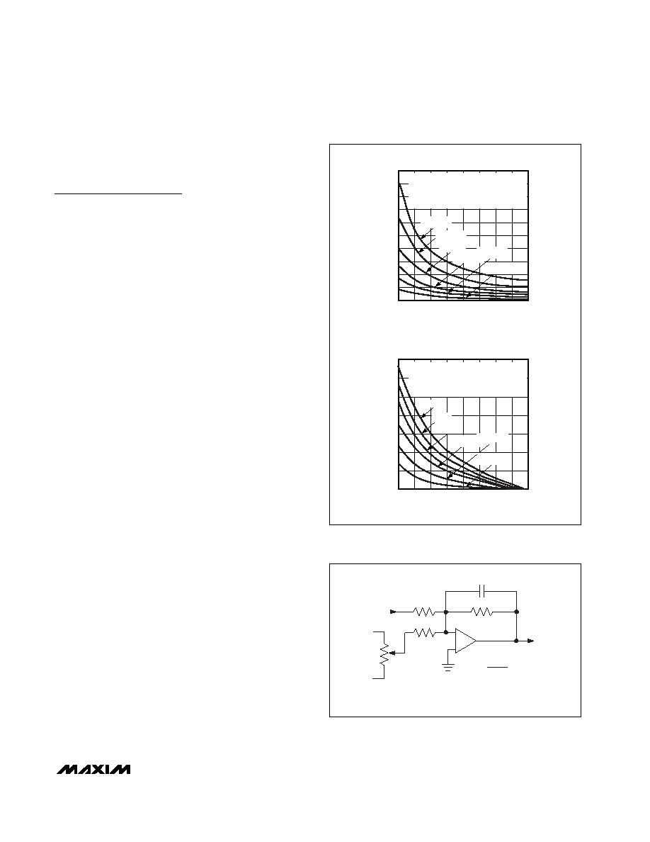
fO ERROR vs. fCLK/fO RATIO (MODE 1, 3)
fCLK/fO RATIO
f O
ERROR
(%)
Q = 0.512
f0 ERROR IS PLOTTED FOR MODES 1 AND 3
MODE 2: MULTIPLY ICLKIO BY
√2 and
DIVIDE Q BY
√2 BEFORE USING GRAPH
MODE 4: MUTIPLY fO ERROR BY 1.5
Q = 0.512
0
-2
-1
-4
-3
-5
-6
-7
40
80
100
60
120 140 160 180 200
Q ERROR vs. fCLK/fO RATIO
fCLK/fO RATIO
Q
ERROR
(%)
Q = 0.5
Q ERROR IS PLOTTED FOR MODES 1 AND 3
MODE 2: MULTIPLY fCLK/fO BY
√2 and
DIVIDE Q BY
√2 BEFORE USING GRAPH
MODE 4: MUTIPLY Q ERROR BY 1.5
Q = 0.83
Q = 7.11
Q = 3.05
Q = 0.6
Q = 1.21
Figure 20. Sampling Errors in fCLK/f0 and Q at Low fCLK/f0 and
Q Settings
R2 100k
R3 270k
VIN
+5V
-5V
OFFSET
TRIM
TO
FILTER
INPUT
100k
+
-
R1 100k
C1
NOTE: OP AMP INCLUDED WITH MAX261/MAX262
GAIN = -R1/R2
fLP =
1
2
πR1C2
Figure 21. Circuit for DC Offset Adjustment
相关PDF资料 |
PDF描述 |
|---|---|
| VE-23Z-IV-S | CONVERTER MOD DC/DC 2V 60W |
| MC9S08SV8CLC | MCU 8BIT 8K FLASH 32-LQFP |
| MC9S08RG60FJE | IC MCU 60K FLASH 8MHZ 32-LQFP |
| MC908QY2AMDWER | MCU 8BIT 1.5K FLASH W/ADC 16SOIC |
| VE-23Y-IX-B1 | CONVERTER MOD DC/DC 3.3V 49.5W |
相关代理商/技术参数 |
参数描述 |
|---|---|
| MAX261BMRG | 功能描述:有源滤波器 RoHS:否 制造商:Maxim Integrated 通道数量:1 截止频率:150 KHz 电源电压-最大:11 V 电源电压-最小:4.74 V 最大工作温度:+ 85 C 安装风格:Through Hole 封装 / 箱体:PDIP N 封装:Tube |
| MAX2620E/D | 制造商:Maxim Integrated Products 功能描述:10MHZ TO 1050MHZ INTEGRATED RF OSCILLATOR WITH BUFFERED OUTP - Gel-pak, waffle pack, wafer, diced wafer on film |
| MAX2620E/D DIE | 制造商:Maxim Integrated Products 功能描述: |
| MAX2620EUA | 功能描述:VCO振荡器 10MHz - 1050MHz RF Oscillator RoHS:否 制造商:Exar 封装 / 箱体:SOIC-14 频率:300 kHz 负载电容: 封装:Reel 电源电压:4.5 V to 20 V 尺寸:4 mm W x 8.75 mm L x 1.75 mm H 最小工作温度:0 C 最大工作温度:+ 70 C |
| MAX2620EUA+ | 功能描述:VCO振荡器 10MHz - 1050MHz RF Oscillator RoHS:否 制造商:Exar 封装 / 箱体:SOIC-14 频率:300 kHz 负载电容: 封装:Reel 电源电压:4.5 V to 20 V 尺寸:4 mm W x 8.75 mm L x 1.75 mm H 最小工作温度:0 C 最大工作温度:+ 70 C |
发布紧急采购,3分钟左右您将得到回复。