- 您现在的位置:买卖IC网 > PDF目录10665 > MAX3062EEKA#TG16 (Maxim Integrated Products)IC TXRX RS485/422 SGL SOT23-8 PDF资料下载
参数资料
| 型号: | MAX3062EEKA#TG16 |
| 厂商: | Maxim Integrated Products |
| 文件页数: | 3/17页 |
| 文件大小: | 0K |
| 描述: | IC TXRX RS485/422 SGL SOT23-8 |
| 产品培训模块: | Lead (SnPb) Finish for COTS Obsolescence Mitigation Program |
| 标准包装: | 1 |
| 类型: | 收发器 |
| 驱动器/接收器数: | 1/1 |
| 规程: | RS422,RS485 |
| 电源电压: | 4.75 V ~ 5.25 V |
| 安装类型: | 表面贴装 |
| 封装/外壳: | SOT-23-8 |
| 供应商设备封装: | SOT-23-8 |
| 包装: | 标准包装 |
| 其它名称: | MAX3062EEKA#TG16DKR |
MAX3060E/MAX3061E/MAX3062E
±15kV ESD-Protected, Fail-Safe, 20Mbps, Slew-Rate-
Limited RS-485/RS-422 Transceivers in a SOT
______________________________________________________________________________________
11
MAX3060E/MAX3061E/MAX3062E
Detailed Description
The MAX3060E/MAX3061E/MAX3062E high-speed trans-
ceivers for RS-485/RS-422 communication contain one
driver and one receiver. These devices feature fail-safe
circuitry, which guarantees a logic-high receiver output
when the receiver inputs are open or shorted, or when
they are connected to a terminated transmission line with
all drivers disabled (see the Fail Safe section). All devices
have a hot-swap input structure that prevents distur-
bances on the differential signal lines when a circuit
board is plugged into a hot backplane (see the Hot-Swap
Capability section). The MAX3060E features a reduced
slew-rate driver that minimizes EMI and reduces reflec-
tions caused by improperly terminated cables, allowing
error-free data transmission up to 115kbps (see the
Reduced EMI and Reflections section). The MAX3061E is
also slew-rate limited, transmitting up to 500kbps. The
MAX3062E driver is not slew-rate limited, allowing trans-
mit speeds up to 20Mbps. The MAX3060E/MAX3061E/
MAX3062E are half-duplex transceivers.
All of these parts operate from a single +5V supply.
Drivers are output short-circuit current limited. Thermal-
shutdown circuitry protects drivers against excessive
power dissipation. When activated, the thermal-shut-
down circuitry places the driver outputs into a high-
impedance state.
Receiver Input Filtering
The receivers of the MAX3060E and MAX3061E incorpo-
rate input filtering in addition to input hysteresis. This fil-
tering enhances noise immunity with differential signals
that have very slow rise and fall times. Receiver propa-
gation delay increases by 2ns due to this filtering.
Fail-Safe
The MAX3060E family of devices guarantee a logic-high
receiver output when the receiver inputs are shorted or
open, or when they are connected to a terminated trans-
mission line with all drivers disabled. This is done by set-
ting the receiver threshold between -50mV and
-200mV. If the differential receiver input voltage (A - B) is
greater than or equal to -50mV, RO is logic high. If
A - B is less than or equal to -200mV, RO is logic low. In
the case of a terminated bus with all transmitters dis-
abled, the receiver’s differential input voltage is pulled to
0V by the termination. In the case of an unterminated bus
with all transmitters disabled, the receiver’s differential
input voltage is pulled to 0V by the receiver’s input resis-
tors. With the receiver thresholds of the MAX3060E fami-
ly, this results in a logic high output with a 50mV
minimum input noise margin. Unlike previous fail-safe
devices, the -50mV to -200mV threshold complies with
the ±200mV EIA/TIA-485 standard.
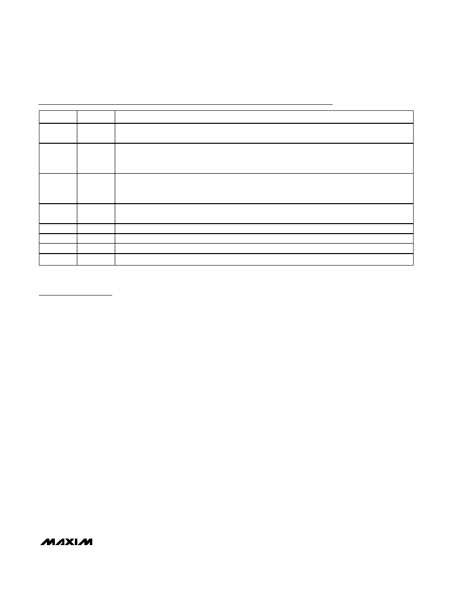
PIN
NAME
FUNCTION
1RO
Receiver Output. When RE is low and when A - B
≥ -50mV, RO is high; if A - B ≤ -200mV, RO is low. RO
is high impedance when RE is high.
2
RE
Receiver Output Enable. Drive RE low to enable RO; RO is high impedance when RE is high. Drive RE
high and DE low to enter low-power shutdown mode. RE is a hot-swap input and reverts to a standard
CMOS input after the first low transition.
3DE
Driver Output Enable. Drive DE high to enable driver outputs. Driver outputs are high impedance when
DE is low. Drive RE high and DE low to enter low-power shutdown mode. DE is a hot-swap input and
reverts to a standard CMOS input after the first high transition.
4DI
Driver Input. With DE high, a low on DI forces the noninverting output low and the inverting output high.
Similarly, a high on DI forces the noninverting output high and the inverting output low.
5
GND
Ground
6
A
Noninverting Receiver Input and Noninverting Driver Output
7
B
Inverting Receiver Input and Inverting Driver Output
8VCC
Positive Supply. Bypass with a 0.1F capacitor to GND.
Pin Description
相关PDF资料 |
PDF描述 |
|---|---|
| VE-B1N-MW | CONVERTER MOD DC/DC 18.5V 100W |
| VI-B1N-MW | CONVERTER MOD DC/DC 18.5V 100W |
| VE-2NR-IX-B1 | CONVERTER MOD DC/DC 7.5V 75W |
| VE-JTP-MY-F4 | CONVERTER MOD DC/DC 13.8V 50W |
| MAX3040CSE+T | IC RS485/422 TRANS QUAD 16-SOIC |
相关代理商/技术参数 |
参数描述 |
|---|---|
| MAX306CPI | 功能描述:多路器开关 IC RoHS:否 制造商:Texas Instruments 通道数量:1 开关数量:4 开启电阻(最大值):7 Ohms 开启时间(最大值): 关闭时间(最大值): 传播延迟时间:0.25 ns 工作电源电压:2.3 V to 3.6 V 工作电源电流: 最大工作温度:+ 85 C 安装风格:SMD/SMT 封装 / 箱体:UQFN-16 |
| MAX306CPI+ | 功能描述:多路器开关 IC 16:1 Precision RoHS:否 制造商:Texas Instruments 通道数量:1 开关数量:4 开启电阻(最大值):7 Ohms 开启时间(最大值): 关闭时间(最大值): 传播延迟时间:0.25 ns 工作电源电压:2.3 V to 3.6 V 工作电源电流: 最大工作温度:+ 85 C 安装风格:SMD/SMT 封装 / 箱体:UQFN-16 |
| MAX306CWI | 功能描述:多路器开关 IC RoHS:否 制造商:Texas Instruments 通道数量:1 开关数量:4 开启电阻(最大值):7 Ohms 开启时间(最大值): 关闭时间(最大值): 传播延迟时间:0.25 ns 工作电源电压:2.3 V to 3.6 V 工作电源电流: 最大工作温度:+ 85 C 安装风格:SMD/SMT 封装 / 箱体:UQFN-16 |
| MAX306CWI+ | 功能描述:多路器开关 IC 16:1 Precision RoHS:否 制造商:Texas Instruments 通道数量:1 开关数量:4 开启电阻(最大值):7 Ohms 开启时间(最大值): 关闭时间(最大值): 传播延迟时间:0.25 ns 工作电源电压:2.3 V to 3.6 V 工作电源电流: 最大工作温度:+ 85 C 安装风格:SMD/SMT 封装 / 箱体:UQFN-16 |
| MAX306CWI+T | 功能描述:多路器开关 IC 16:1 Precision RoHS:否 制造商:Texas Instruments 通道数量:1 开关数量:4 开启电阻(最大值):7 Ohms 开启时间(最大值): 关闭时间(最大值): 传播延迟时间:0.25 ns 工作电源电压:2.3 V to 3.6 V 工作电源电流: 最大工作温度:+ 85 C 安装风格:SMD/SMT 封装 / 箱体:UQFN-16 |
发布紧急采购,3分钟左右您将得到回复。