- 您现在的位置:买卖IC网 > PDF目录9863 > MAX3346EEBE+T (Maxim Integrated Products)IC USB TXRX ESD PROTECT 16-UCSP PDF资料下载
参数资料
| 型号: | MAX3346EEBE+T |
| 厂商: | Maxim Integrated Products |
| 文件页数: | 10/17页 |
| 文件大小: | 0K |
| 描述: | IC USB TXRX ESD PROTECT 16-UCSP |
| 产品培训模块: | Lead (SnPb) Finish for COTS Obsolescence Mitigation Program |
| 标准包装: | 2,500 |
| 类型: | 收发器 |
| 驱动器/接收器数: | 1/1 |
| 规程: | USB 2.0 |
| 电源电压: | 4 V ~ 5.5 V |
| 安装类型: | 表面贴装 |
| 封装/外壳: | 16-WFBGA,CSPBGA |
| 供应商设备封装: | 16-UCSP(2x2) |
| 包装: | 带卷 (TR) |
MAX3346E
±15kV ESD-Protected USB Transceiver
in UCSP
2
_______________________________________________________________________________________
ABSOLUTE MAXIMUM RATINGS
Stresses beyond those listed under “Absolute Maximum Ratings” may cause permanent damage to the device. These are stress ratings only, and functional
operation of the device at these or any other conditions beyond those indicated in the operational sections of the specifications is not implied. Exposure to
absolute maximum rating conditions for extended periods may affect device reliability.
Supply Voltage (VCC) ...............................................-0.3V to +6V
Output of Internal Regulator (VTRM) ..........-0.3V to (VCC + 0.3V)
Input Voltage (D+, D-) ..............................................-0.3V to +6V
System Supply Voltage (VL) .....................................-0.3V to +6V
RCV, SUSP, VM, VP, MODE,
OE, SPEED, ENUM ....................................-0.3V to (VL + 0.3V)
Short-Circuit Current (D+, D-)
to VCC or GND (Note 1) ..........................................Continuous
Maximum Continuous Current (all other pins) ..................±15mA
Continuous Power Dissipation (TA = +70°C)
4 x 4 UCSP (derate 7.4mW/°C above +70°C).....589mW [B16-2]
14-Pin TSSOP (derate 9.1mW/°C above +70°C) ..727mW [U14-1]
Operating Temperature Range ...........................-40°C to +85°C
Junction Temperature ......................................................+150°C
Storage Temperature Range .............................-65°C to +150°C
Lead Temperature (soldering, 10s) .................................+300°C
Bump Temperature (soldering) Reflow............................+235°C
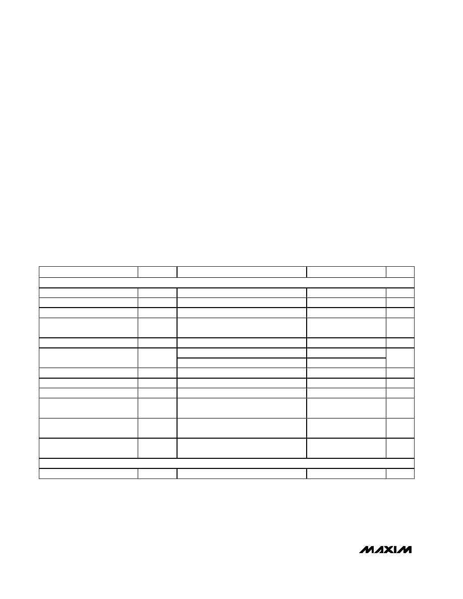
PARAMETER
SYMBOL
CONDITIONS
MIN
TYP
MAX
UNITS
SUPPLY INPUTS (VCC, VTRM, VL)
Regulated Supply Voltage
VVTRM
Internal regulator
3.0
3.3
3.6
V
VL Input Range
1.65
3.60
V
VCC Input Range
4.0
5.5
V
Operating VCC Supply Current
IVCC
Full-speed transmitting/receiving at
12Mbps, CL = 50pF on D+ and D-
8mA
Operating VL Supply Current
IVL
Full-speed transmitting/receiving at 12Mbps
6mA
Full-speed idle: VD+ > 2.7V, VD- < 0.3V
340
450
Full-Speed Idle and SE0 Supply
Current
IVCC(IDLE)
SE0: VD+ < 0.3V, VD- < 0.3V
390
500
A
Static VL Supply Current
IVL(STATIC)
Full-speed idle, SE0, or suspend mode
5
A
Suspend Supply Current
IVCC(SUSP)
SUSP = OE = high
40
A
Disable-Mode Supply Current
IVCC(DIS)
VL = GND or open
20
A
D+/D- Disable-Mode
Load Current
ID_(DIS)
VL = GND or open, VD_ = 0 or +5.5V
5
A
Sharing-Mode VL Supply
Current
IVL(SHARING)
VCC = GND or open, OE = low,
SUSP = high
20
A
D+/D- Sharing-Mode
Load Current
ID_(SHARING) VCC = GND or open, VD_ = 0 or +5.5V
20
A
LINEAR REGULATOR
External Capacitor
COUT
Compensation of linear regulator
1
F
(All voltages referenced to GND, unless otherwise noted.)
Note 1: External 23.7 resistors connected to D+ and D-.
ELECTRICAL CHARACTERISTICS
(VCC = +4V to +5.5V, GND = 0, VTRM = +3.0V to +3.6V, VL = +1.65V to +3.6V, TA = TMIN to TMAX, unless otherwise noted. Typical
values are at VCC = +5V, VL = +2.5V, TA = +25°C.) (Note 2)
相关PDF资料 |
PDF描述 |
|---|---|
| MS27467E15B35PA | CONN PLUG 37POS STRAIGHT W/PINS |
| MAX3190EEUT+T | IC RS-232 TRANSMITTER SOT23-6 |
| MS3102R14S-2SY | CONN RCPT 4POS BOX MNT W/SCKT |
| MS3102R14S-2SX | CONN RCPT 4POS BOX MNT W/SCKT |
| ICL7109CPL+2 | IC ADC 12BIT 3-ST 40-DIP |
相关代理商/技术参数 |
参数描述 |
|---|---|
| MAX3346EEUD | 功能描述:USB 接口集成电路 RoHS:否 制造商:Cypress Semiconductor 产品:USB 2.0 数据速率: 接口类型:SPI 工作电源电压:3.15 V to 3.45 V 工作电源电流: 最大工作温度:+ 85 C 安装风格:SMD/SMT 封装 / 箱体:WLCSP-20 |
| MAX3346EEUD+ | 功能描述:USB 接口集成电路 ESD-Protected USB Tcvr RoHS:否 制造商:Cypress Semiconductor 产品:USB 2.0 数据速率: 接口类型:SPI 工作电源电压:3.15 V to 3.45 V 工作电源电流: 最大工作温度:+ 85 C 安装风格:SMD/SMT 封装 / 箱体:WLCSP-20 |
| MAX3346EEUD+T | 功能描述:USB 接口集成电路 ESD-Protected USB Tcvr RoHS:否 制造商:Cypress Semiconductor 产品:USB 2.0 数据速率: 接口类型:SPI 工作电源电压:3.15 V to 3.45 V 工作电源电流: 最大工作温度:+ 85 C 安装风格:SMD/SMT 封装 / 箱体:WLCSP-20 |
| MAX3346EEUD-T | 功能描述:USB 接口集成电路 RoHS:否 制造商:Cypress Semiconductor 产品:USB 2.0 数据速率: 接口类型:SPI 工作电源电压:3.15 V to 3.45 V 工作电源电流: 最大工作温度:+ 85 C 安装风格:SMD/SMT 封装 / 箱体:WLCSP-20 |
| MAX3349EAEBE+ | 制造商:Maxim Integrated Products 功能描述: |
发布紧急采购,3分钟左右您将得到回复。