- 您现在的位置:买卖IC网 > PDF目录10659 > MAX3362EKA#TG16 (Maxim Integrated Products)IC TXRX RS485/422 SGL SOT23-8 PDF资料下载
参数资料
| 型号: | MAX3362EKA#TG16 |
| 厂商: | Maxim Integrated Products |
| 文件页数: | 2/14页 |
| 文件大小: | 0K |
| 描述: | IC TXRX RS485/422 SGL SOT23-8 |
| 产品培训模块: | Lead (SnPb) Finish for COTS Obsolescence Mitigation Program |
| 标准包装: | 1 |
| 类型: | 收发器 |
| 驱动器/接收器数: | 1/1 |
| 规程: | RS422,RS485 |
| 电源电压: | 3.14 V ~ 3.47 V |
| 安装类型: | 表面贴装 |
| 封装/外壳: | SOT-23-8 |
| 供应商设备封装: | SOT-23-8 |
| 包装: | 标准包装 |
| 其它名称: | MAX3362EKA#TG16DKR |
MAX3362
3.3V, High-Speed, RS-485/RS-422 Transceiver in
SOT Package
10
______________________________________________________________________________________
The MAX3362 has a 1/8-unit-load receiver input imped-
ance, allowing up to 256 transceivers to be connected
simultaneously on a bus. The MAX3362 is designed for
half-duplex communication.
Driver
The driver transfers single-ended input (DI) to differen-
tial outputs (A, B). The driver enable (DE) input controls
the driver. When DE is high, driver outputs are enabled.
These outputs are high impedance when DE is low.
When the driver is enabled, setting DI low forces the
noninverting output (A) low and inverting output (B)
high. Conversely, drive DI high to force noninverting
output high and inverting output low (Table 1).
Drive RE high and DE low (disable both receiver and
driver outputs) to enter low-power shutdown mode.
Receiver
The receiver reads differential inputs from the bus lines
(A, B) and transfers this data as a single-ended output
(RO). The receiver enable (RE) input controls the
receiver. Drive RE low to enable the receiver. Driving
RE high places RO into a high-impedance state.
When the receiver is enabled, RO is high if (A-B)
≥
200mV. RO is low if (A-B)
≤ -200mV.
Drive RE high and DE low (disable both receiver and
driver outputs) to enter low-power shutdown mode.
Hot-Swap Capability
Hot-Swap Input
When circuit boards are inserted into a hot or powered
backplane, disturbances to the enable and differential
receiver inputs can lead to data errors. Upon initial cir-
cuit board insertion, the processor undergoes its
power-up sequence. During this period, the output dri-
vers are high impedance and are unable to drive the
DE input of the MAX3362 to a defined logic level.
Leakage currents up to 10A from the high-impedance
output could cause DE to drift to an incorrect logic
state. Additionally, parasitic circuit board capacitance
could cause coupling of VCC or GND to DE. These fac-
tors could improperly enable the driver.
When VCC rises, an internal pulldown circuit holds DE
low for at least 10s and until the current into DE
exceeds 200A. After the initial power-up sequence,
the pulldown circuit becomes transparent, resetting the
hot-swap tolerable input.
Hot-Swap Input Circuitry
The MAX3362 enable inputs feature hot-swap capability.
At the input there are two NMOS devices, M1 and M2
(Figure 8). When VCC ramps from 0, an internal 10s
timer turns on M2 and sets the SR latch, which also turns
on M1. Transistors M2, a 300A current sink, and M1, a
30A current sink, pull DE to GND through an 8k
Ω resis-
tor. M2 is designed to pull DE to the disabled state
against an external parasitic capacitance up to 100pF
that may drive DE high. After 10s, the timer deactivates
M2 while M1 remains on, holding DE low against three-
state leakages that may drive DE high. M1 remains on
until an external source overcomes the required input
current. At this time, the SR latch resets and M1 turns off.
When M1 turns off, DE reverts to a standard, high-
impedance CMOS input. Whenever VCC drops below
1V, the hot-swap input is reset.
For RE there is a complementary circuit employing two
PMOS devices pulling RE to VCC.
Hot-Swap Line Transient
The circuit of Figure 9 shows a typical offset termination
used to guarantee a greater than 200mV offset when a
line is not driven (the 50pF represents the minimum
parasitic capacitance that would exist in a typical appli-
cation). During a hot-swap event when the driver is
TRANSMITTING
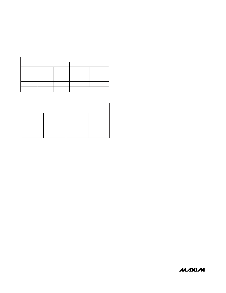
INPUTS
OUTPUTS
RE
DE
DI
A
B
X1
1
0
X1
0
1
0
X
High Z
1
0
X
Shutdown
Table 1. Transmitter Functional Table
RECEIVING
INPUTS
OUTPUT
RE
DE
A – B
RO
0X
≥ 200mV
1
0X
≤ -200mV
0
1
X
High-Z
1
0
X
Shutdown
Table 2. Receiver Functional Table
相关PDF资料 |
PDF描述 |
|---|---|
| VI-J1L-MW-F3 | CONVERTER MOD DC/DC 28V 100W |
| AD1674ARZ | IC ADC 12BIT 100KSPS 28-SOIC |
| AD7693BRMZ | IC ADC 16BIT 500KSPS 10-MSOP |
| VI-J1L-MW-F2 | CONVERTER MOD DC/DC 28V 100W |
| LTC1419CSW#PBF | IC A/D CONV 14BIT SAMPLNG 28SOIC |
相关代理商/技术参数 |
参数描述 |
|---|---|
| MAX336C/D | 功能描述:多路器开关 IC RoHS:否 制造商:Texas Instruments 通道数量:1 开关数量:4 开启电阻(最大值):7 Ohms 开启时间(最大值): 关闭时间(最大值): 传播延迟时间:0.25 ns 工作电源电压:2.3 V to 3.6 V 工作电源电流: 最大工作温度:+ 85 C 安装风格:SMD/SMT 封装 / 箱体:UQFN-16 |
| MAX336C/D DIE | 制造商:Maxim Integrated Products 功能描述: |
| MAX336CAI | 功能描述:多路器开关 IC RoHS:否 制造商:Texas Instruments 通道数量:1 开关数量:4 开启电阻(最大值):7 Ohms 开启时间(最大值): 关闭时间(最大值): 传播延迟时间:0.25 ns 工作电源电压:2.3 V to 3.6 V 工作电源电流: 最大工作温度:+ 85 C 安装风格:SMD/SMT 封装 / 箱体:UQFN-16 |
| MAX336CAI+ | 功能描述:多路器开关 IC 16:1 Low Leakage CMOS MUX RoHS:否 制造商:Texas Instruments 通道数量:1 开关数量:4 开启电阻(最大值):7 Ohms 开启时间(最大值): 关闭时间(最大值): 传播延迟时间:0.25 ns 工作电源电压:2.3 V to 3.6 V 工作电源电流: 最大工作温度:+ 85 C 安装风格:SMD/SMT 封装 / 箱体:UQFN-16 |
| MAX336CAI+T | 功能描述:多路器开关 IC 16:1 Low Leakage CMOS MUX RoHS:否 制造商:Texas Instruments 通道数量:1 开关数量:4 开启电阻(最大值):7 Ohms 开启时间(最大值): 关闭时间(最大值): 传播延迟时间:0.25 ns 工作电源电压:2.3 V to 3.6 V 工作电源电流: 最大工作温度:+ 85 C 安装风格:SMD/SMT 封装 / 箱体:UQFN-16 |
发布紧急采购,3分钟左右您将得到回复。