- 您现在的位置:买卖IC网 > PDF目录2088 > MAX3625ACUG+T (Maxim Integrated Products)IC CLOCK GENERATOR PREC 24-TSSOP PDF资料下载
参数资料
| 型号: | MAX3625ACUG+T |
| 厂商: | Maxim Integrated Products |
| 文件页数: | 7/10页 |
| 文件大小: | 0K |
| 描述: | IC CLOCK GENERATOR PREC 24-TSSOP |
| 产品培训模块: | Lead (SnPb) Finish for COTS Obsolescence Mitigation Program |
| 标准包装: | 2,500 |
| 类型: | 时钟发生器 |
| PLL: | 带旁路 |
| 输入: | LVCMOS,晶体 |
| 输出: | LVPECL |
| 电路数: | 1 |
| 比率 - 输入:输出: | 2:3 |
| 差分 - 输入:输出: | 无/是 |
| 频率 - 最大: | 318.75MHz |
| 除法器/乘法器: | 是/无 |
| 电源电压: | 3 V ~ 3.6 V |
| 工作温度: | 0°C ~ 70°C |
| 安装类型: | 表面贴装 |
| 封装/外壳: | 24-TSSOP(0.173",4.40mm 宽) |
| 供应商设备封装: | 24-TSSOP |
| 包装: | 带卷 (TR) |
MAX3625A
Low-Jitter, Precision Clock
Generator with Three Outputs
6
_______________________________________________________________________________________
Detailed Description
The MAX3625A is a low-jitter clock generator designed
to operate at Ethernet and Fibre Channel frequencies. It
consists of an on-chip crystal oscillator, PLL, program-
mable dividers, and LVPECL output buffers. Using a
low-frequency clock (crystal or CMOS input) as a refer-
ence, the internal PLL generates a high-frequency out-
put clock with excellent jitter performance.
Crystal Oscillator
An integrated oscillator provides the low-frequency ref-
erence clock for the PLL. This oscillator requires an
external crystal connected between X_IN and X_OUT.
The crystal frequency is 24.8MHz to 27MHz.
REF_IN Buffer
An LVCMOS-compatible clock source can be connect-
ed to REF_IN to serve as the reference clock.
The LVCMOS REF_IN buffer is internally biased to the
threshold voltage (1.4V typ) to allow AC- or DC-cou-
pling, and is designed to operate up to 320MHz.
PLL
The PLL takes the signal from the crystal oscillator or
reference clock input and synthesizes a low-jitter, high-
frequency clock. The PLL contains a phase-frequency
detector (PFD), a lowpass filter, and a voltage-con-
trolled oscillator (VCO) with a 620MHz to 648MHz oper-
ating range. The VCO is connected to the PFD input
through a feedback divider. See Table 3 for divider val-
ues. The PFD compares the reference frequency to the
divided-down VCO output (fVCO/M) and generates a
control signal that keeps the VCO locked to the refer-
ence clock. The high-frequency VCO output clock is
sent to the output dividers. To minimize noise-induced
jitter, the VCO supply (VCCA) is isolated from the core
logic and output buffer supplies.
Output Dividers
The output dividers are programmable to allow a range of
output frequencies. See Table 2 for the divider input set-
tings. The output dividers are automatically set to divide by
1 when the MAX3625A is in bypass mode (BYPASS = 0).
LVPECL Drivers
The high-frequency outputs—QA, QB0, and QB1—are
differential PECL buffers designed to drive transmission
lines terminated with 50
Ω to VCC - 2.0V. The maximum
operating frequency is specified up to 320MHz. The
outputs can be disabled, if not used. The outputs go to
a logic 0 when disabled.
Reset Logic/POR
During power-on, a power-on reset (POR) signal is gen-
erated to synchronize all dividers. An external master
reset (MR) signal is not required.
Applications Information
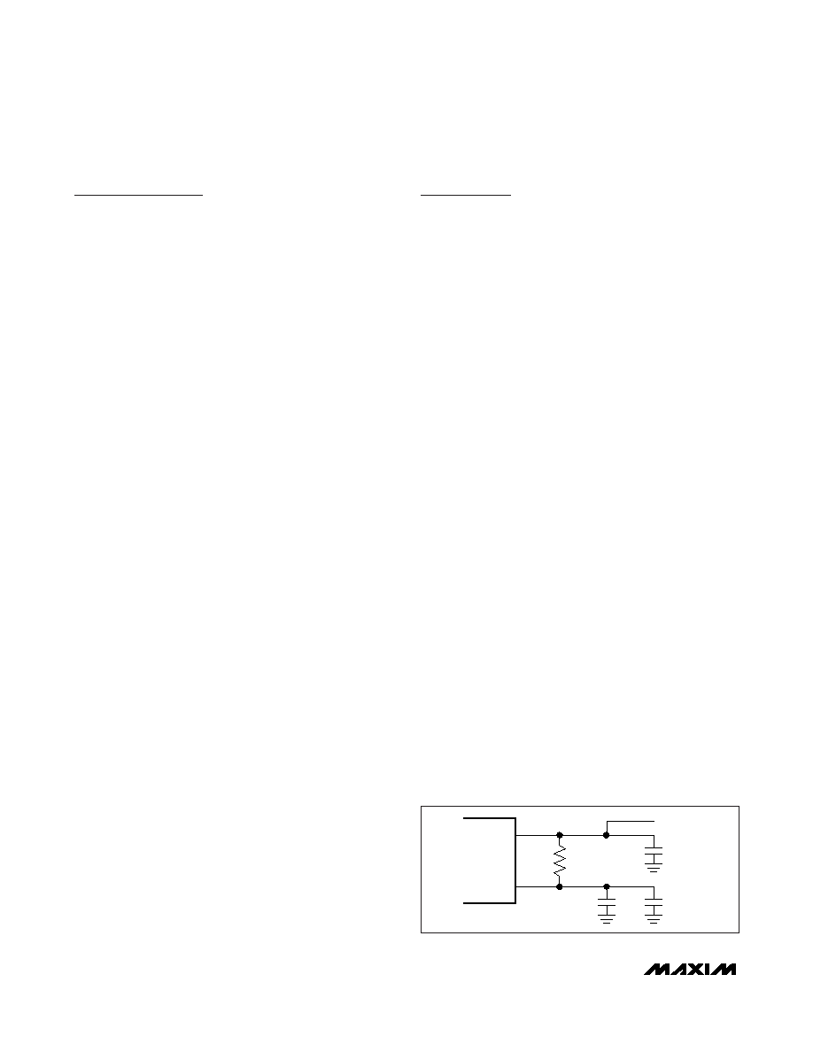
Power-Supply Filtering
The MAX3625A is a mixed analog/digital IC. The PLL
contains analog circuitry susceptible to random noise.
In addition to excellent on-chip power-supply noise
rejection, the MAX3625A provides a separate power-
supply pin, VCCA, for the VCO circuitry. Figure 1 illus-
trates the recommended power-supply filter network for
VCCA. The purpose of this design technique is to
ensure a clean power supply to the VCO circuitry and
to improve the overall immunity to power-supply noise.
This network requires that the power supply is +3.3V
±5%. Decoupling capacitors should be used on all
supply pins for best performance.
Output Divider Configuration
Table 2 shows the input settings required to set the out-
put dividers. Note that when the MAX3625A is in
bypass mode (BYPASS set low), the output dividers are
automatically set to divide by 1.
PLL Divider Configuration
Table 3 shows the input settings required to set the PLL
feedback divider.
Crystal Selection
The crystal oscillator is designed to drive a fundamen-
tal mode, AT-cut crystal resonator. See Table 4 for rec-
ommended crystal specifications. See Figure 3 for
external capacitance connection.
Crystal Input Layout
The crystal, trace, and two external capacitors should
be placed on the board as close as possible to the
MAX3625A’s X_IN and X_OUT pins to reduce crosstalk
of active signals into the oscillator. The example layout
shown in Figure 2 gives approximately 3pF of trace
plus footprint capacitance per side of the crystal. The
dielectric material is FR-4 and dielectric thickness of
the reference board is 15 mils. Using a 25MHz crystal
and the capacitor values of C10 = 27pF and C9 =
33pF, the measured output frequency accuracy is
-14ppm at +25°C ambient temperature.
VCC
VCCA
10.5
Ω
+3.3V
±5%
0.01
μF
10
μF
0.01
μF
Figure 1. Analog Supply Filtering
相关PDF资料 |
PDF描述 |
|---|---|
| MAX3625BEUG+T | IC CLOCK GENERATOR PREC 24TSSOP |
| MAX3645EEE+T | IC AMP LIMITING 16-QSOP |
| MAX3654ETE+T | IC AMP TRANSIMPEDANCE 16-TQFN |
| MAX3658AETA+T | IC AMP TRANSIMPEDANCE 8-TDFN |
| MAX3660ETE+T | IC TRANSIMPEDANCE AMP 16TQFN-EP |
相关代理商/技术参数 |
参数描述 |
|---|---|
| MAX3625BEUG+ | 功能描述:时钟发生器及支持产品 Low Jitter Precision w/Four Outputs RoHS:否 制造商:Silicon Labs 类型:Clock Generators 最大输入频率:14.318 MHz 最大输出频率:166 MHz 输出端数量:16 占空比 - 最大:55 % 工作电源电压:3.3 V 工作电源电流:1 mA 最大工作温度:+ 85 C 安装风格:SMD/SMT 封装 / 箱体:QFN-56 |
| MAX3625BEUG+T | 功能描述:时钟发生器及支持产品 Low Jitter Precision w/Four Outputs RoHS:否 制造商:Silicon Labs 类型:Clock Generators 最大输入频率:14.318 MHz 最大输出频率:166 MHz 输出端数量:16 占空比 - 最大:55 % 工作电源电压:3.3 V 工作电源电流:1 mA 最大工作温度:+ 85 C 安装风格:SMD/SMT 封装 / 箱体:QFN-56 |
| MAX3625BEVKIT+ | 功能描述:时钟发生器及支持产品 Not Available From Mouser RoHS:否 制造商:Silicon Labs 类型:Clock Generators 最大输入频率:14.318 MHz 最大输出频率:166 MHz 输出端数量:16 占空比 - 最大:55 % 工作电源电压:3.3 V 工作电源电流:1 mA 最大工作温度:+ 85 C 安装风格:SMD/SMT 封装 / 箱体:QFN-56 |
| MAX3625CUG+ | 功能描述:时钟发生器及支持产品 Not Available From Mouser RoHS:否 制造商:Silicon Labs 类型:Clock Generators 最大输入频率:14.318 MHz 最大输出频率:166 MHz 输出端数量:16 占空比 - 最大:55 % 工作电源电压:3.3 V 工作电源电流:1 mA 最大工作温度:+ 85 C 安装风格:SMD/SMT 封装 / 箱体:QFN-56 |
| MAX3625CUG+T | 功能描述:时钟发生器及支持产品 Not Available From Mouser RoHS:否 制造商:Silicon Labs 类型:Clock Generators 最大输入频率:14.318 MHz 最大输出频率:166 MHz 输出端数量:16 占空比 - 最大:55 % 工作电源电压:3.3 V 工作电源电流:1 mA 最大工作温度:+ 85 C 安装风格:SMD/SMT 封装 / 箱体:QFN-56 |
发布紧急采购,3分钟左右您将得到回复。