- 您现在的位置:买卖IC网 > PDF目录20066 > MAX3656ETG+T (Maxim Integrated)IC LASR DRVR 2.5GBPS 3.6V 24TQFN PDF资料下载
参数资料
| 型号: | MAX3656ETG+T |
| 厂商: | Maxim Integrated |
| 文件页数: | 4/15页 |
| 文件大小: | 0K |
| 描述: | IC LASR DRVR 2.5GBPS 3.6V 24TQFN |
| 产品培训模块: | Lead (SnPb) Finish for COTS Obsolescence Mitigation Program |
| 标准包装: | 1 |
| 类型: | 激光二极管驱动器(光纤) |
| 数据速率: | 2.5Gbps |
| 通道数: | 1 |
| 电源电压: | 3 V ~ 3.6 V |
| 电流 - 电源: | 40mA |
| 电流 - 调制: | 85mA |
| 电流 - 偏置: | 70mA |
| 工作温度: | -40°C ~ 85°C |
| 封装/外壳: | 24-WFQFN 裸露焊盘 |
| 供应商设备封装: | 24-TQFN-EP(4x4) |
| 包装: | 标准包装 |
| 安装类型: | 表面贴装 |
| 产品目录页面: | 1423 (CN2011-ZH PDF) |
| 其它名称: | MAX3656ETG+TDKR |
�� �
�
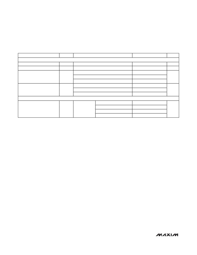
�155Mbps� to� 2.5Gbps� Burst-Mode�
�Laser� Driver�
�ELECTRICAL� CHARACTERISTICS� (continued)�
�(Typical� values� are� at� V� CC� =� +3.3V,� I� BIAS� =� 20mA,� I� MOD� =� 25mA,� extinction� ratio� =� 10dB,� and� T� A� =� +25� °� C,� unless� otherwise� noted.)�
�PARAMETER�
�SYMBOL�
�CONDITIONS�
�MIN�
�TYP�
�MAX�
�UNITS�
�BURST-MODE� SPECIFICATIONS�
�Burst� Enable� Delay�
�Burst� Disable� Delay�
�APC� closed� loop� (Notes� 10,� 11,� 13)�
�APC� closed� loop� (Notes� 10,� 12,� 13)�
�155Mbps�
�2881�
�2.3�
�2.0�
�ns�
�ns�
�Burst� On-Time� (Note� 13)�
�t� B-ON�
�622Mbps�
�720�
�ns�
�1.25Gbps,� 2.5Gbps�
�155Mbps�
�576�
�192�
�Burst� Off-Time� (Note� 13)�
�t� B-OFF�
�622Mbps�
�96�
�ns�
�OPTICAL� EVALUATION�
�1.25Gbps,� 2.5Gbps�
�96�
�ExceLight�
�155.52Mbps�
�45�
�Optical� Eye� Diagram� Mask�
�Margin�
�SLT2886-LR�
�laser� diode�
�(or� equivalent)�
�622.08Mbps�
�1.24416Gbps�
�2.48832Gbps�
�40�
�31�
�24�
�%�
�Note� 1:� Excludes� I� BIAS� and� I� MOD� .� Maximum� value� is� specified� at� I� MOD� =� 85mA,� I� BIAS� =� 70mA,� and� I� MD� =� 1.5mA.�
�Note� 2:� For� safety� purposes,� both� the� bias� and� modulation� currents� are� switched� off� if� any� of� the� current� set� pins� (BIASMAX,� MODSET)�
�are� grounded.�
�Note� 3:� Accuracy� refers� to� part-to-part� variation.�
�Note� 4:� APC� loop� initialization� definitions:�
�I� BIAS� Error:� I� BIAS� -� I� BIASSET� ,� where� I� BIAS� =� the� actual� bias� current� and� I� BIASSET� =� the� level� of� bias� current� set� by� the� R� APCSET�
�resistor.�
�Initialization� Case� 1:� Continuous� Mode� Power-Up.� In� this� case,� EN� =� low,� BEN� =� high,� and� then� V� CC� is� ramped� up� from�
�0V� to� ≥� 3.0V.�
�Initialization� Case� 2:� Chip-Enable� Reset.� In� this� case,� 3.0V� ≤� V� CC� ≤� 3.6V,� BEN� =� high,� and� then� EN� changes� from� high� to� low.�
�Initialization� Case� 3:� Burst-Mode� Startup.� In� this� case,� 3.0V� ≤� V� CC� ≤� 3.6V,� EN� =� low,� and� then� BEN� changes� from� low� to� high.�
�Note� 5:� I� BIAS� error� is� less� than� 3.8mA� (for� an� extinction� ratio� of� 10dB� and� I� MD� =� 1500μA)� within� 12μs� from� the� time� that� V� CC� ≥� 3.0V.�
�Note� 6:� I� BIAS� error� is� less� than� 3.8mA� (for� an� extinction� ratio� of� 10dB� and� I� MD� =� 1500μA)� within� 2.1μs� (typ)� from� the� time� that� EN� <� 0.8V.�
�Note� 7:� I� BIAS� error� must� be� less� than� 3.8mA� (for� an� extinction� ratio� of� 10dB� and� I� MD� =� 1500μA)� at� or� before� the� end� of� the� third�
�burst� following� the� transition� of� BEN� from� low� to� high.� For� the� shortest� burst� on-� and� off-time� (576ns� and� 96ns),� this� trans-�
�lates� to� 1.92μs� from� when� BEN� toggles� from� low� to� high� for� the� first� time� after� startup.�
�Note� 8:� Rise� and� fall� times� are� measured� as� 20%� to� 80%� of� the� output� amplitude� with� a� repeating� 0000011111.�
�Note� 9:� Deterministic� jitter� is� measured� with� a� continuous� data� pattern� (no� bursting)� of� 2� 7� -� 1� PRBS� +� 80� consecutive� ones� +� 2� 7� -� 1�
�PRBS� +� 80� consecutive� zeros.�
�Note� 10:� Measured� electrically� with� a� resistive� load� matched� to� the� laser� driver� output.�
�Note� 11:� Enable� delay� is� measured� between� (1)� the� time� at� which� the� rising� edge� of� the� differential� burst� enable� input� signal� reach-�
�es� the� midpoint� of� the� voltage� swing,� and� (2)� the� time� at� which� the� combined� output� currents� (bias� and� modulation)� reach�
�90%� of� the� final� level� set� by� R� APCSET� ,� R� BIASMAX� ,� and� R� MODSET� (after� all� transients� such� as� overshoot,� ringing,� etc.,� have�
�settled� to� within� 10%� of� their� final� values).� See� Figure� 1.� Measurement� done� for� 10mA� ≤� I� MOD� ≤� 85mA� and� 4mA� ≤� I� BIAS� ≤�
�70mA.�
�Note� 12:� Disable� delay� is� measured� between� (1)� the� time� at� which� the� falling� edge� of� the� differential� burst� enable� input� signal� reaches�
�the� midpoint� of� the� voltage� swing,� and� (2)� the� time� at� which� the� combined� output� currents� (bias� and� modulation)� fall� below�
�10%� of� the� bias� on� current� (after� transients� have� settled).� See� Figure� 1.� Measurement� done� for� 10mA� ≤� I� MOD� ≤� 85mA� and�
�4mA� ≤� I� BIAS� ≤� 70mA.�
�Note� 13:� Guaranteed� by� design� and� characterization.�
�4�
�_______________________________________________________________________________________�
�相关PDF资料 |
PDF描述 |
|---|---|
| VY2150K29U2JS63V5 | CAP CER 15PF 300V 10% RADIAL |
| NH35BP-2F10 | BATTERY PACK NIMH 12.0V 2500MAH |
| EMA36DTMZ-S664 | CONN EDGECARD 72POS R/A .125 SLD |
| GRM1885C1H5R0CZ01D | CAP CER 5PF 50V NP0 0603 |
| EBC20DRTI | CONN EDGECARD 40POS DIP .100 SLD |
相关代理商/技术参数 |
参数描述 |
|---|---|
| MAX3656EVKIT | 功能描述:激光驱动器 Evaluation Kit for the MAX3656 RoHS:否 制造商:Micrel 数据速率:4.25 Gbps 工作电源电压:3 V to 3.6 V 电源电流:80 mA 最大工作温度:+ 85 C 封装 / 箱体:QFN-16 封装:Tube |
| MAX3656EVKIT+ | 功能描述:电源管理IC开发工具 MAX3656 Eval Kit RoHS:否 制造商:Maxim Integrated 产品:Evaluation Kits 类型:Battery Management 工具用于评估:MAX17710GB 输入电压: 输出电压:1.8 V |
| MAX3657BE/D | 功能描述:跨阻抗放大器 RoHS:否 制造商:Texas Instruments 封装 / 箱体:SOIC-14 带宽:3 MHz 工作电源电压:36 V 电源电流:5.5 mA 工作温度范围:- 40 C to + 85 C 封装:Tube |
| MAX3657BE/D DIE | 制造商:Maxim Integrated Products 功能描述: |
| MAX3657E/D | 功能描述:跨阻抗放大器 RoHS:否 制造商:Texas Instruments 封装 / 箱体:SOIC-14 带宽:3 MHz 工作电源电压:36 V 电源电流:5.5 mA 工作温度范围:- 40 C to + 85 C 封装:Tube |
发布紧急采购,3分钟左右您将得到回复。