- 您现在的位置:买卖IC网 > PDF目录5331 > MAX366CPA+ (Maxim Integrated Products)IC CIRCUIT PROT SIGNAL-LINE 8DIP PDF资料下载
参数资料
| 型号: | MAX366CPA+ |
| 厂商: | Maxim Integrated Products |
| 文件页数: | 8/12页 |
| 文件大小: | 0K |
| 描述: | IC CIRCUIT PROT SIGNAL-LINE 8DIP |
| 产品培训模块: | Lead (SnPb) Finish for COTS Obsolescence Mitigation Program |
| 标准包装: | 50 |
| 电压 - 箝位: | ±40V |
| 技术: | 混合技术 |
| 功率(瓦特): | 727mW |
| 电路数: | 3 |
| 应用: | 通用 |
| 封装/外壳: | 8-DIP(0.300",7.62mm) |
| 供应商设备封装: | 8-PDIP |
| 包装: | 管件 |
�� �
�
�Signal-Line� Circuit� Protectors�
�Bipolar� Faults�
�The� MAX366/MAX367� V+� and� V-� pins� are� normally� con-�
�nected� to� a� circuit’s� most� positive� and� most� negative�
�power� supplies.� When� a� circuit� has� multiple� power�
�supplies� (such� as� ±5V� and� ±12V)� and� the� MAX366/�
�+5V�
�MAX367� V+� and� V-� pins� are� connected� to� the� lower�
�supply,� it� is� possible� to� have� fault� conditions� on� both�
�sides� of� the� signal� path� at� once,� if� both� sides� of� the�
�switch� have� paths� to� higher� voltages.� If� the� polarity� of�
�1�
�IN1�
�MAX366�
�V+�
�OUT1�
�8�
�7�
�10� μ� F�
�100k�
�these� faults� is� the� same,� the� signal� path� will� be� open�
�and� there� is� no� conflict.�
�2�
�IN2�
�OUT2�
�6�
�If� the� IN� and� OUT� pins� are� driven� in� opposite� polarities�
�from� low-impedance� sources,� the� lower� of� the� two�
�3�
�IN3�
�OUT3�
�5�
�OP� AMP�
�impedances� will� overcome� the� higher� impedance,� just�
�as� if� the� protector� were� not� present.� (Make� sure� the�
�current� does� not� exceed� the� 30mA� absolute� maximum�
�rating.)� As� the� lower� impedance� source� approaches�
�4�
�V-�
�and� exceeds� the� fault� knee� voltage,� the� protector� will�
�conduct� enough� current� to� maintain� the� other� signal� pin�
�near� the� fault� knee� voltage.� This� means� when� the� fault�
�knee� voltage� is� reached,� the� current� through� the� pro-�
�tector� shifts� from� the� higher� current� capability� of� the�
�10� μ� F�
�100k�
�-5V�
�lower� impedance� source� to� the� lower� current� capability�
�of� the� higher� impedance� source.�
�_______________Typical� Applications�
�Driven� Switches�
�The� MAX366/MAX367� have� low� supply� currents�
�(<1μA),� which� allows� the� supply� pins� to� be� driven�
�directly� by� other� active� circuitry,� instead� of� connected�
�directly� to� the� power� sources.� In� this� configuration,�
�the� parts� can� be� used� as� driven� fault-protected�
�switches� with� V+� or� V-� pins� used� as� the� control� pins.�
�For� example,� if� the� V-� pin� is� grounded,� you� can� turn�
�the� V+� pin� on� and� off� by� driving� it� with� the� output� of� a�
�CMOS� gate.� This� effectively� connects� and� discon-�
�nects� three� or� eight� separate� signal� lines� at� once.� (If�
�bipolar� signals� or� signals� that� go� to� ground� are� being�
�switched,� the� V-� pin� must� be� driven� simultaneously� to�
�a� negative� potential.)� Always� ensure� that� the� driving�
�source(s)� does� not� drive� the� V+� pin� more� negative�
�than� the� V-� pin.�
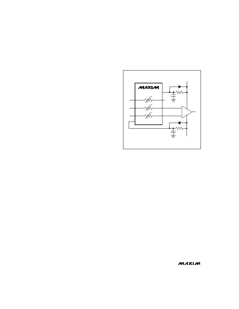
�Figure� 4� shows� a� simple� turn-on� delay� that� takes�
�advantage� of� the� MAX366’s� low� power� consumption.�
�The� two� RC� networks� cause� gradual� application� of�
�power� to� the� MAX366,� which� in� turn� applies� the� input�
�signals� smoothly� after� the� amplifier� has� stabilized.�
�The� two� diodes� discharge� the� two� capacitors� rapidly�
�when� power� is� turned� off.�
�Figure� 4.� Turn-On� Delay�
�This� circuit� can� be� tailored� to� nearly� any� rate� of� turn-�
�on� by� selecting� the� RC� time� constants� in� the� V+� and�
�V-� pins,� without� affecting� the� time� constant� of� the�
�measuring� circuit.�
�Protectors� as� Circuit� Elements�
�Any� of� the� individual� protectors� in� a� MAX366� or� MAX367�
�may� be� used� as� a� switched� resistor,� independent� of� the�
�functions� of� other� elements� in� the� same� package.� For�
�example,� Figure� 5� shows� a� MAX366� with� two� of� the� pro-�
�tectors� used� to� protect� the� input� of� an� op� amp,� and� the�
�third� element� used� to� sequence� a� power� supply.�
�Combining� the� circuits� of� Figures� 4� and� 5� produces� a�
�delayed� action� on� the� switched� +5V,� as� well� as� smooth�
�application� of� signals� to� the� amplifier� input.�
�_________Testing� Circuit� Protectors�
�Measuring� Path� Resistance�
�Measuring� path� resistance� requires� special� techniques,�
�since� path� resistance� varies� dramatically� with� the� IN�
�and� OUT� voltages� relative� to� the� supply� voltages.�
�Conventional� ohmmeters� should� not� be� used,� for� two�
�reasons:� 1)� the� applied� voltage� and� currents� are� usual-�
�ly� not� predictable,� and� 2)� the� true� resistance� is� a� func-�
�tion� of� the� applied� voltage,� which� is� dramatically� altered�
�by� the� ohmmeter� itself.� Autoranging� ohmmeters� are�
�particularly� unreliable.�
�8�
�_______________________________________________________________________________________�
�相关PDF资料 |
PDF描述 |
|---|---|
| EL8403IU | IC OP AMP 500MHZ R-R 16-QSOP |
| 7100.1114.13 | FUSE 800MA 250V T-LAG 19MM PCB |
| B2050CCLRP | BATTRAX SLIC DUAL NEG 500A DO214 |
| RGH2012-2E-P-512-B | RES 5.1K OHM .1% 1/4W 0805 SMD |
| ADG465BRTZ-REEL7 | IC CHANNEL PROTECTOR SGL SOT23-6 |
相关代理商/技术参数 |
参数描述 |
|---|---|
| MAX366CPA+ | 功能描述:隔离器接口集成电路 Signal Line Circuit Protector RoHS:否 制造商:Texas Instruments 通道数量:2 传播延迟时间: 电源电压-最大:5.5 V 电源电压-最小:3 V 电源电流:3.6 mA 功率耗散: 最大工作温度:+ 125 C 安装风格: 封装 / 箱体:SOIC-8 封装:Tube |
| MAX366CSA | 功能描述:TVS二极管阵列 RoHS:否 制造商:Littelfuse 极性: 通道:4 Channels 击穿电压: 钳位电压:11.5 V 工作电压:2.5 V 峰值浪涌电流:20 A 安装风格:SMD/SMT 端接类型:SMD/SMT 系列: 最小工作温度:- 40 C 最大工作温度:+ 85 C |
| MAX366CSA+ | 功能描述:隔离器接口集成电路 Signal Line Circuit Protector RoHS:否 制造商:Texas Instruments 通道数量:2 传播延迟时间: 电源电压-最大:5.5 V 电源电压-最小:3 V 电源电流:3.6 mA 功率耗散: 最大工作温度:+ 125 C 安装风格: 封装 / 箱体:SOIC-8 封装:Tube |
| MAX366CSA+T | 功能描述:隔离器接口集成电路 Signal Line Circuit Protector RoHS:否 制造商:Texas Instruments 通道数量:2 传播延迟时间: 电源电压-最大:5.5 V 电源电压-最小:3 V 电源电流:3.6 mA 功率耗散: 最大工作温度:+ 125 C 安装风格: 封装 / 箱体:SOIC-8 封装:Tube |
| MAX366CSA-T | 功能描述:TVS二极管阵列 RoHS:否 制造商:Littelfuse 极性: 通道:4 Channels 击穿电压: 钳位电压:11.5 V 工作电压:2.5 V 峰值浪涌电流:20 A 安装风格:SMD/SMT 端接类型:SMD/SMT 系列: 最小工作温度:- 40 C 最大工作温度:+ 85 C |
发布紧急采购,3分钟左右您将得到回复。