- 您现在的位置:买卖IC网 > PDF目录1940 > MAX3892ETH+T (Maxim Integrated Products)IC 4:1 SERIALIZER SONET 44-TQFN PDF资料下载
参数资料
| 型号: | MAX3892ETH+T |
| 厂商: | Maxim Integrated Products |
| 文件页数: | 6/11页 |
| 文件大小: | 0K |
| 描述: | IC 4:1 SERIALIZER SONET 44-TQFN |
| 产品培训模块: | Lead (SnPb) Finish for COTS Obsolescence Mitigation Program |
| 标准包装: | 2,500 |
| 功能: | 串行器 |
| 数据速率: | 2.7Gbps |
| 输入类型: | LVDS |
| 输出类型: | CML |
| 输入数: | 4 |
| 输出数: | 1 |
| 电源电压: | 3 V ~ 3.6 V |
| 工作温度: | -40°C ~ 85°C |
| 安装类型: | 表面贴装 |
| 封装/外壳: | 44-WFQFN 裸露焊盘 |
| 供应商设备封装: | 44-TQFN-EP(7x7) |
| 包装: | 带卷 (TR) |
MAX3892
+3.3V, 2.5Gbps/2.7Gbps, SDH/SONET 4:1
Serializer with Clock Synthesis
4
_______________________________________________________________________________________
Note 1: Specifications at -40°C are guaranteed by design and characterization.
Note 2: Measured with SLBO/CLK622 and SCLK outputs disabled and CML outputs open.
Note 3: AC characteristics are guaranteed by design and characterization.
Note 4: In 622MHz clock mode, the parallel data is clocked in by the rising edge of the 622MHz/666MHz parallel clock input. In the
311MHz clock mode, the parallel data is clocked in on both the rising and falling edges of the clock. The parallel input
setup and hold time increases by 60ps if the duty cycle is between 48% to 52% in 311MHz mode (Figure 1).
Note 5: Relative to the falling edge of the SCLKO.
Note 6: Measurement bandwidth is BW = 12kHz to 20MHz.
Note 7: Measured with 00001111 pattern, RCLK to PCLKI/PDI[3:0] phase approximately 40ps. See the
Jitter Generation vs. RCLK to
PCLK/PDI[3:0] Phase plot in the Typical Operating Characteristics section.
Note 8: Deterministic jitter includes pattern-dependent jitter and pulse-width distortion. Measured using a 27 - 1 PRBS pattern with
96 consecutive identical digits.
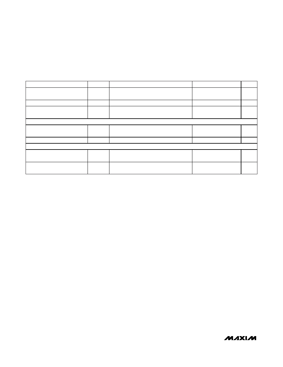
AC ELECTRICAL CHARACTERISTICS (continued)
(VCC = +3.0V to +3.6V, TA = -40°C to +85°C. Typical values are at VCC = +3.3V, differential LVDS loads = 100
Ω ±1%, CML loads =
50
Ω ±1%, TA = +25°C, unless otherwise noted.) (Note 3)
PARAMETER
SYMBOL
CONDITIONS
MIN
TYP
MAX
UNITS
Serial Clock Output Jitter
Generation
JG
(Notes 6 and 7)
1.0
1.4
psRMS
Serial Data Output Random Jitter
RJ
(Note 7)
1.4
psRMS
Serial Data Output Deterministic
Jitter
DJ
(Note 8)
19
psP-P
REFERENCE CLOCK INPUT SPECIFICATIONS (RCLK)
Reference Clock Frequency
Tolerance
±100
ppm
Reference Clock Input Duty Cycle
30
70
%
RESET INPUTS (RESET)
Minimum Pulse Width of FIFO
Reset
UI is PCLKO period
4
UI
Tolerated Drift Between PCLKI
and PCLKO After Reset
UI is PCLKO period
±1UI
相关PDF资料 |
PDF描述 |
|---|---|
| MAX392ESE | IC SWITCH QUAD SPST 16SOIC |
| MAX3941ETG+T | IC EAM DRIVER 10GBPS 24-TQFN |
| MAX3942ETG+T | IC MODULATOR DRVR 10GBPS 24-TQFN |
| MAX394EAP | IC SWITCH QUAD SPDT 20SSOP |
| MAX395EAG+T | IC SWITCH OCTAL SPST 24SSOP |
相关代理商/技术参数 |
参数描述 |
|---|---|
| MAX389C/D | 功能描述:多路器开关 IC RoHS:否 制造商:Texas Instruments 通道数量:1 开关数量:4 开启电阻(最大值):7 Ohms 开启时间(最大值): 关闭时间(最大值): 传播延迟时间:0.25 ns 工作电源电压:2.3 V to 3.6 V 工作电源电流: 最大工作温度:+ 85 C 安装风格:SMD/SMT 封装 / 箱体:UQFN-16 |
| MAX389CJN | 功能描述:多路器开关 IC RoHS:否 制造商:Texas Instruments 通道数量:1 开关数量:4 开启电阻(最大值):7 Ohms 开启时间(最大值): 关闭时间(最大值): 传播延迟时间:0.25 ns 工作电源电压:2.3 V to 3.6 V 工作电源电流: 最大工作温度:+ 85 C 安装风格:SMD/SMT 封装 / 箱体:UQFN-16 |
| MAX389CPN | 功能描述:多路器开关 IC RoHS:否 制造商:Texas Instruments 通道数量:1 开关数量:4 开启电阻(最大值):7 Ohms 开启时间(最大值): 关闭时间(最大值): 传播延迟时间:0.25 ns 工作电源电压:2.3 V to 3.6 V 工作电源电流: 最大工作温度:+ 85 C 安装风格:SMD/SMT 封装 / 箱体:UQFN-16 |
| MAX389CPN+ | 功能描述:多路器开关 IC 8:2 8Ch Fault Prtcd Analog MUX RoHS:否 制造商:Texas Instruments 通道数量:1 开关数量:4 开启电阻(最大值):7 Ohms 开启时间(最大值): 关闭时间(最大值): 传播延迟时间:0.25 ns 工作电源电压:2.3 V to 3.6 V 工作电源电流: 最大工作温度:+ 85 C 安装风格:SMD/SMT 封装 / 箱体:UQFN-16 |
| MAX389CWG | 功能描述:多路器开关 IC RoHS:否 制造商:Texas Instruments 通道数量:1 开关数量:4 开启电阻(最大值):7 Ohms 开启时间(最大值): 关闭时间(最大值): 传播延迟时间:0.25 ns 工作电源电压:2.3 V to 3.6 V 工作电源电流: 最大工作温度:+ 85 C 安装风格:SMD/SMT 封装 / 箱体:UQFN-16 |
发布紧急采购,3分钟左右您将得到回复。