- 您现在的位置:买卖IC网 > PDF目录8621 > MAX3964AETP+ (Maxim Integrated Products)IC AMP LIMITING SGNL DET 20-TQFN PDF资料下载
参数资料
| 型号: | MAX3964AETP+ |
| 厂商: | Maxim Integrated Products |
| 文件页数: | 7/11页 |
| 文件大小: | 0K |
| 描述: | IC AMP LIMITING SGNL DET 20-TQFN |
| 产品培训模块: | Lead (SnPb) Finish for COTS Obsolescence Mitigation Program |
| 标准包装: | 75 |
| 类型: | 限幅放大器 |
| 应用: | 光纤学网络 |
| 安装类型: | 表面贴装 |
| 封装/外壳: | 20-WFQFN 裸露焊盘 |
| 供应商设备封装: | 20-TQFN-EP(4x4) |
| 包装: | 管件 |
MAX3964A/MAX3968
+3.0V to +5.5V, 125Mbps to 266Mbps
Limiting Amplifiers with Loss-of-Signal Detector
_______________________________________________________________________________________
5
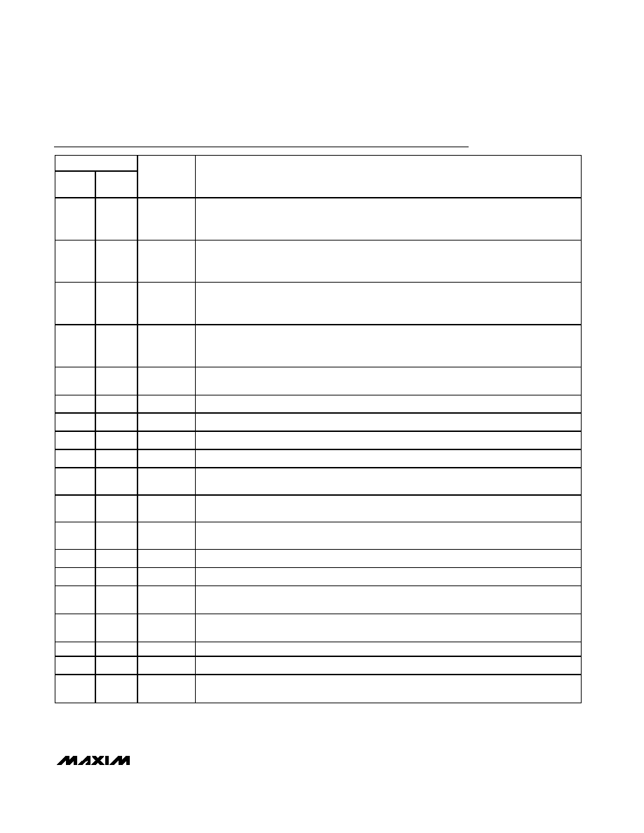
Pin Description
PIN
QSOP
THIN
QFN
NAME
FUNCTION
1
19
SQUELCH
Squelch Input. The squelch function disables the data outputs by forcing OUT- low and OUT+
high during a loss-of-signal condition. Connect to GND or leave unconnected to disable.
Connect to VCC to enable squelching.
2
20
VTH
Output of Internal Op Amp that Sets Loss-of-Signal Threshold Voltage (Figure 1). Connect a
resistor from VTH to INV and from INV to ground (minimum resistance 100k) to program the
desired threshold voltage.
3
1
INV
Inverting Input of Internal Op Amp that Sets Loss-of-Signal Threshold Voltage (Figure 1).
Connect a resistor from VTH to INV and from INV to ground (minimum resistance 100k) to
program the desired threshold voltage.
4
2
FILTER
Filter Output of Full-Wave Logarithmic Detectors (FWDs). The FWD outputs are summed
together at FILTER to generate the received-signal-strength indicator (RSSI). Connect a
capacitor from FILTER to VCC for proper operation.
5
3
RSSI
Received-Signal-Strength Indicator Output. The analog DC voltage at RSSI indicates the input
signal power. The RSSI output is reduced approximately 120mV when LOS+ is asserted.
6
4
IN-
Inverting Data Input
7
5
IN+
Noninverting Data Input
8
—
SUB
Substrate. Connect to ground.
9, 10
6, 7, 8
GND
Ground
11
9
CZP
Auto-Zero Capacitor Input. Connect a capacitor between CZP and CZN to determine the offset-
correction-loop bandwidth.
12
10
CZN
Auto-Zero Capacitor Input. Connect a capacitor between CZP and CZN to determine the offset-
correction-loop bandwidth.
13
11
VCCO
Output Buffer Supply Voltage. Connect to the same potential as VCC, but filter VCCO and VCC
separately.
14
12
OUT+
Noninverting PECL Data Output. Terminate with 50 to (VCC - 2V).
15
13
OUT-
Inverting PECL Data Output. Terminate with 50 to (VCC - 2V).
16
14
LOS-
Inverting Loss-of-Signal Output. LOS- is asserted low when input power drops below the LOS
threshold. This pin is PECL compatible and should be terminated with 50 to (VCC - 2V).
17
15
LOS+
Noninverting Loss-of-Signal Output. LOS+ is asserted high when input power drops below the
LOS threshold. This pin is PECL compatible and should be terminated with 50 to (VCC - 2V).
18
16
VCCO
MAX3964A/MAX3968: This pin can be left open or connected to the positive supply.
19, 20
17, 18
VCC
+3.0V to +5.5V Supply Voltage
—EP
Exposed
Pad
Connect the exposed pad to board ground for optional electrical and thermal performance.
相关PDF资料 |
PDF描述 |
|---|---|
| MAX9001EUB+ | IC OP AMP LP HI SPEED 10-UMAX |
| AD9717BCPZRL7 | IC DAC DUAL 14BIT LO PWR 40LFCSP |
| MAX9000EUA+ | IC OP AMP LP HI SPEED 8-UMAX |
| AD5065BRUZ-REEL7 | IC DAC DUAL 16BIT SPI 14TSSOP |
| LTC2753ACUK-16#PBF | IC DAC 16BIT DUAL 48-QFN |
相关代理商/技术参数 |
参数描述 |
|---|---|
| MAX3964AETP+ | 功能描述:限幅放大器 3-5.5V 125-266Mbps Limiting Amp RoHS:否 制造商:Micrel 输入电压范围(最大值):3.6 V 工作电源电压:3.3 V 电源电流:40 mA 工作温度范围:- 40 C to + 85 C 封装 / 箱体:MSOP-10 封装:Tube |
| MAX3964AETP+T | 功能描述:限幅放大器 3-5.5V 125-266Mbps Limiting Amp RoHS:否 制造商:Micrel 输入电压范围(最大值):3.6 V 工作电源电压:3.3 V 电源电流:40 mA 工作温度范围:- 40 C to + 85 C 封装 / 箱体:MSOP-10 封装:Tube |
| MAX3964AETP-T | 功能描述:限幅放大器 3-5.5V 125-266Mbps Limiting Amp RoHS:否 制造商:Micrel 输入电压范围(最大值):3.6 V 工作电源电压:3.3 V 电源电流:40 mA 工作温度范围:- 40 C to + 85 C 封装 / 箱体:MSOP-10 封装:Tube |
| MAX3964C/D DIE | 制造商:Maxim Integrated Products 功能描述: |
| MAX3964CEP | 制造商:Maxim Integrated Products 功能描述:+3.0V TO +5.5V, 125MBPS TO 266MBPS LINITING A - Bulk |
发布紧急采购,3分钟左右您将得到回复。