- 您现在的位置:买卖IC网 > PDF目录2088 > MAX3969ETP+T (Maxim Integrated Products)IC AMP LIMIT 200MBPS 20-TQFN PDF资料下载
参数资料
| 型号: | MAX3969ETP+T |
| 厂商: | Maxim Integrated Products |
| 文件页数: | 7/11页 |
| 文件大小: | 0K |
| 描述: | IC AMP LIMIT 200MBPS 20-TQFN |
| 产品培训模块: | Lead (SnPb) Finish for COTS Obsolescence Mitigation Program |
| 标准包装: | 2,500 |
| 类型: | 限幅放大器 |
| 应用: | 光纤学网络 |
| 安装类型: | 表面贴装 |
| 封装/外壳: | 20-WFQFN 裸露焊盘 |
| 供应商设备封装: | 20-TQFN-EP(4x4) |
| 包装: | 带卷 (TR) |
MAX3969
200Mbps SFP Limiting Amplifier
_______________________________________________________________________________________
5
Pin Description
PIN
NAME
FUNCTION
17, 18
VCC
Supply Voltage
19
SQUELCH
Squelch Input. The squelch function disables the data outputs by forcing OUT- low and OUT+ high
when the signal is below the power-detect threshold. Connect to GND or leave unconnected to
disable squelch. Connect to VCC to enable squelch.
20
VTH
Output of Internal Op Amp that Sets Power-Detect Threshold Voltage (Figure 1). Connect a resistor
from VTH to INV (R2) and from INV to ground (R1 = 100k
Ω), to program the desired threshold voltage.
EP
Exposed
Pad
Ground. The exposed pad must be soldered to the circuit board ground for proper thermal and
electrical performance.
OFFSET
CORRECTION
1
O
1.2V
REFERENCE
CIN
IN+
FILTER
VCC
IN-
FWD
CFILTER
CAZ
CZN
CZP
R1
100k
Ω
R2
INV
VTH
VCC
VCCO
GND
OUT-
OUT+
SQUELCH
RSSI
LOS
SD
MAX3969
PECL
TTL
PECL
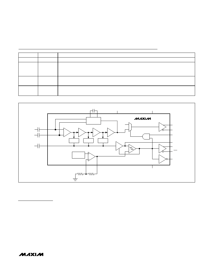
Figure 1. Functional Diagram
Detailed Description
The MAX3969 contains a series of limiting amplifiers
and power detectors, offset correction, data-squelch
circuitry, TTL buffers for LOS outputs, and PECL output
buffers for signal detect (SD) and data outputs. See
Figure 1 for the functional diagram.
Gain Stages and Offset Correction
A cascade of limiting amplifiers provides approximately
65dB of combined small-signal gain. The large gain
makes the amplifier susceptible to small DC offsets in
the signal path. To correct DC offsets, the amplifier has
an internal feedback loop that acts as a DC autozero
circuit. By correcting the DC offsets, the limiting amplifi-
er sensitivity and power-detector accuracy are
improved.
The offset correction is optimized for data streams with
a 50% duty cycle. A different average duty cycle results
in increased pulse-width distortion and loss of sensitivi-
ty. The offset-correction circuitry is less sensitive to vari-
ations of input duty cycle (for example, the 40% to 60%
duty cycle encountered in 4B/5B coding) when the
input is less than 30mVP-P.
The data inputs must be AC-coupled for the offset cor-
rection loop to function properly. Differential input
impedance is >5k
Ω.
相关PDF资料 |
PDF描述 |
|---|---|
| MAX3971AUTP+T | IC AMP LIMIT 10.7GBPS 20-TQFN |
| MAX4025EUP+ | IC AMP VIDEO MUX 2:1 20-TSSOP |
| MAX4027ESD+T | IC AMP VIDEO MUX 2CH 14-SOIC |
| MAX4029EUP+ | IC AMP VIDEO MUX 2:1 20-TSSOP |
| MAX4031EESD+ | IC OP AMP TRPL 144MHZ 14-SOIC |
相关代理商/技术参数 |
参数描述 |
|---|---|
| MAX396C/D | 功能描述:多路器开关 IC RoHS:否 制造商:Texas Instruments 通道数量:1 开关数量:4 开启电阻(最大值):7 Ohms 开启时间(最大值): 关闭时间(最大值): 传播延迟时间:0.25 ns 工作电源电压:2.3 V to 3.6 V 工作电源电流: 最大工作温度:+ 85 C 安装风格:SMD/SMT 封装 / 箱体:UQFN-16 |
| MAX396CAI | 功能描述:多路器开关 IC RoHS:否 制造商:Texas Instruments 通道数量:1 开关数量:4 开启电阻(最大值):7 Ohms 开启时间(最大值): 关闭时间(最大值): 传播延迟时间:0.25 ns 工作电源电压:2.3 V to 3.6 V 工作电源电流: 最大工作温度:+ 85 C 安装风格:SMD/SMT 封装 / 箱体:UQFN-16 |
| MAX396CAI+ | 功能描述:多路器开关 IC 16:1 Precision Analog MUX RoHS:否 制造商:Texas Instruments 通道数量:1 开关数量:4 开启电阻(最大值):7 Ohms 开启时间(最大值): 关闭时间(最大值): 传播延迟时间:0.25 ns 工作电源电压:2.3 V to 3.6 V 工作电源电流: 最大工作温度:+ 85 C 安装风格:SMD/SMT 封装 / 箱体:UQFN-16 |
| MAX396CAI+T | 功能描述:多路器开关 IC 16:1 Precision Analog MUX RoHS:否 制造商:Texas Instruments 通道数量:1 开关数量:4 开启电阻(最大值):7 Ohms 开启时间(最大值): 关闭时间(最大值): 传播延迟时间:0.25 ns 工作电源电压:2.3 V to 3.6 V 工作电源电流: 最大工作温度:+ 85 C 安装风格:SMD/SMT 封装 / 箱体:UQFN-16 |
| MAX396CAI-T | 功能描述:多路器开关 IC RoHS:否 制造商:Texas Instruments 通道数量:1 开关数量:4 开启电阻(最大值):7 Ohms 开启时间(最大值): 关闭时间(最大值): 传播延迟时间:0.25 ns 工作电源电压:2.3 V to 3.6 V 工作电源电流: 最大工作温度:+ 85 C 安装风格:SMD/SMT 封装 / 箱体:UQFN-16 |
发布紧急采购,3分钟左右您将得到回复。